Application
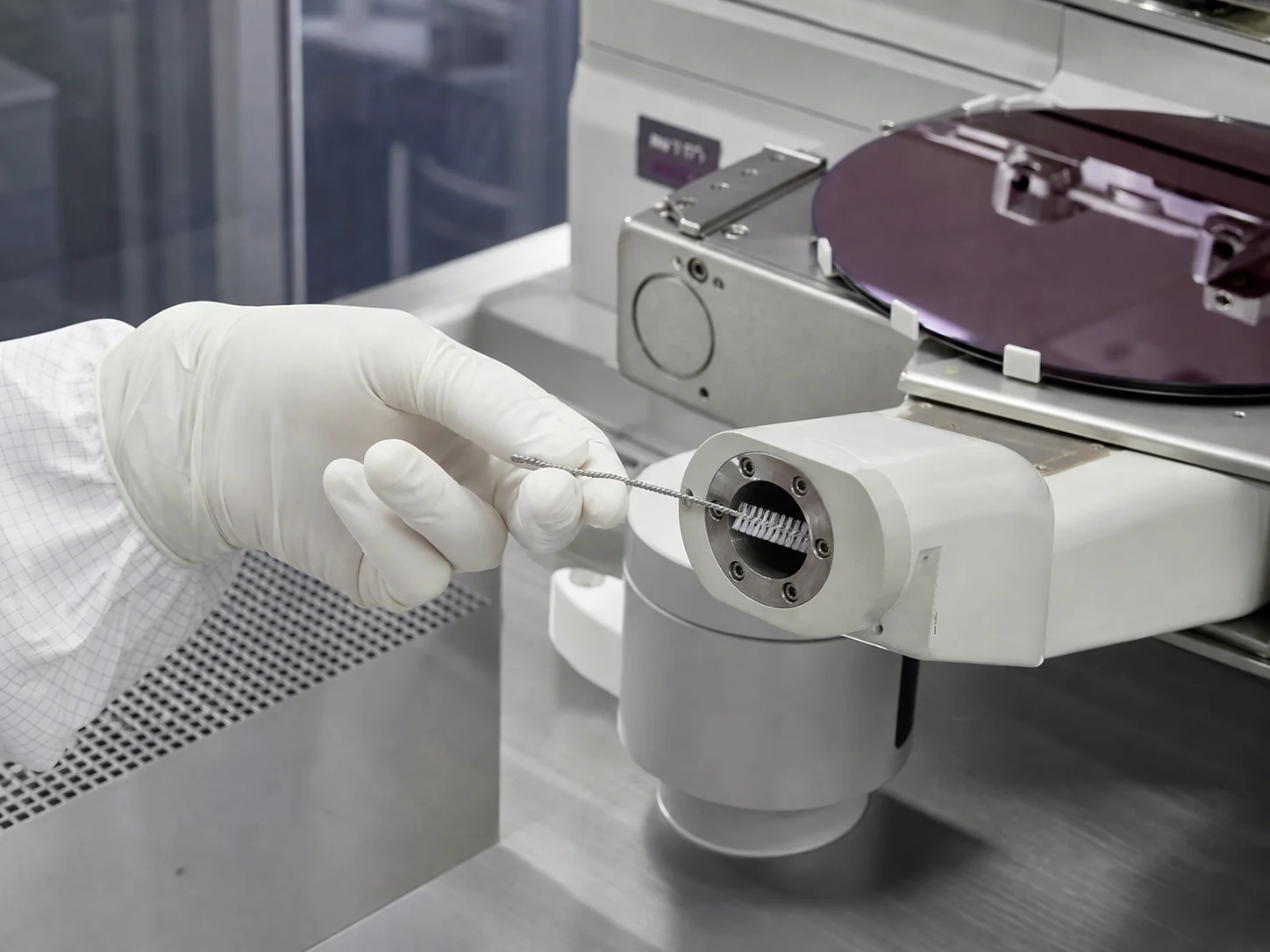
Semiconductor Wafer Handling End-effector Cleaning
For Semiconductor Wafer Handling End-effector Cleaning, the brush must reach the working area, disturb or collect particles/abrasive slurry/organic film/silicon dust, and release it without creating unacceptable surface damage or process interference. Choose the brush structure from the available access, contact direction, and cleaning process.
Application Overview
Semiconductor Wafer Handling End-effector Cleaning connects contaminant type, required stiffness, temperature, chemical exposure, compliance and working environment to brush material and geometry.
The selection sequence for Semiconductor Wafer Handling End-effector Cleaning starts with the access path and contact direction, then checks how the residue breaks free and leaves the work zone. The service environment is Cleanroom / ESD-Controlled Area. The cleaning method is Dry Brushing / Wet Brushing / Ultrasonic Cleaning. Confirm temperature (150°C), chemical exposure (Ultrapure Water; Isopropyl Alcohol; Mild Acids and Alkalis pH 5–9), and documentation or compliance (ISO 14644-1 Cleanliness Classification; SEMI S2; Low Particles / Low Ions / Low Outgassing) before finalizing the material and construction. The mapped product set uses powered motion, so the machine interface and customer-supplied operating conditions must be confirmed.
Common Challenges
Primary project question
Which brush material, geometry and cleaning method can remove Particles/Abrasive Slurry/Organic Film/Silicon Dust under the stated temperature, chemical and environmental conditions?
Operating conditions
For Semiconductor Wafer Handling End-effector Cleaning, confirm required contact level (Soft), maximum stated temperature (150°C), chemical exposure (Ultrapure Water; Isopropyl Alcohol; Mild Acids and Alkalis pH 5–9), and documentation or compliance (ISO 14644-1 Cleanliness Classification; SEMI S2; Low Particles / Low Ions / Low Outgassing).
Failure prevention
For Semiconductor Wafer Handling End-effector Cleaning, verify access, installed engagement, contact direction, and the path for releasing particles/abrasive slurry/organic film/silicon dust before increasing filament stiffness, density, or applied force. Choose another cleaning method when brush contact cannot reach the deposit or achieve the required result.
Selection and Project Inputs
For Semiconductor Wafer Handling End-effector Cleaning, confirm the working area, residue, access opening or clearance, contact motion, acceptable surface condition, and the path for removing loosened material. Enter the required dimensions and operating conditions in the table below.
| Contaminant | Particles/Abrasive Slurry/Organic Film/Silicon Dust |
|---|---|
| Required hardness | Soft |
| Maximum temperature | 150°C |
| Chemical exposure | Ultrapure Water; Isopropyl Alcohol; Mild Acids and Alkalis pH 5–9 |
| Cleaning method | Dry Brushing/Wet Brushing/Ultrasonic Cleaning |
| Environment | Cleanroom/ESD-Controlled Area |
Continue Exploring
Recommended Reading & Related Brush Resources
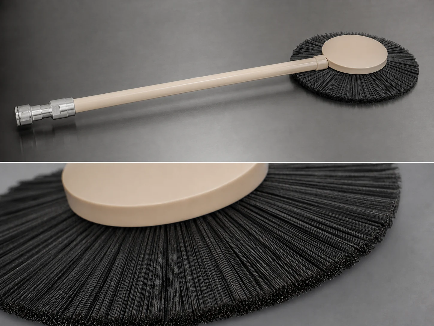
150mm Carbon Fiber Wafer Equipment Disc Brush
Custom 150mm Carbon Fiber Wafer Equipment Disc Brush using CARBON-FIBER contact material, 150 mm…
Review product specifications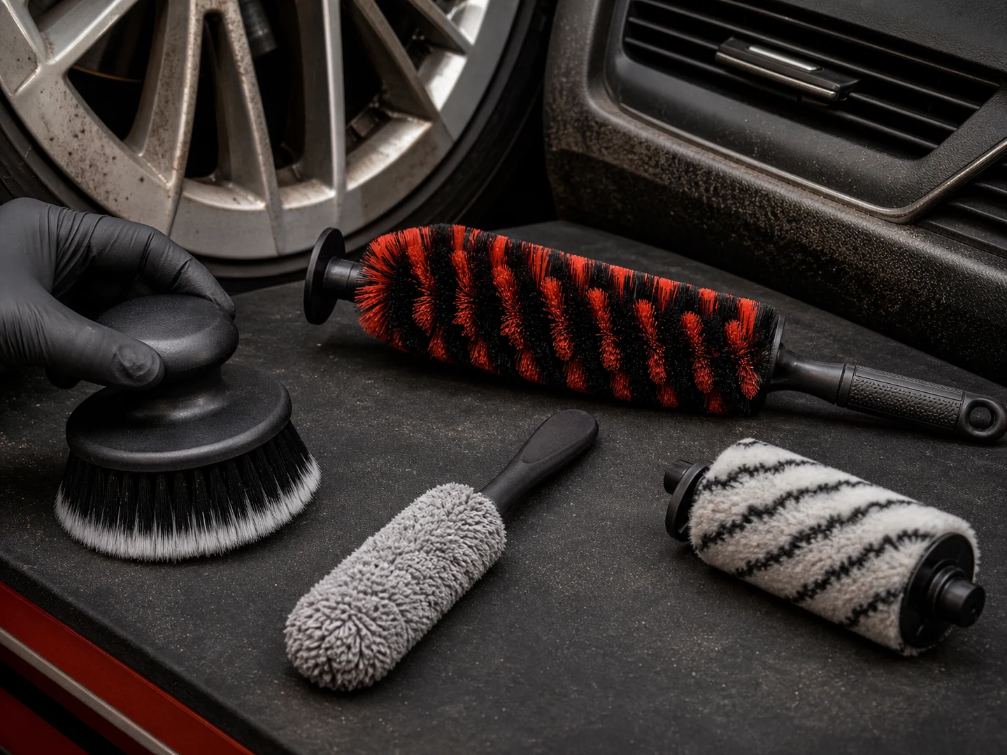
Custom Handheld Detail Brushes
Choose a handheld detail brush when the operator needs direct control in seams, recesses,…
Explore this brush type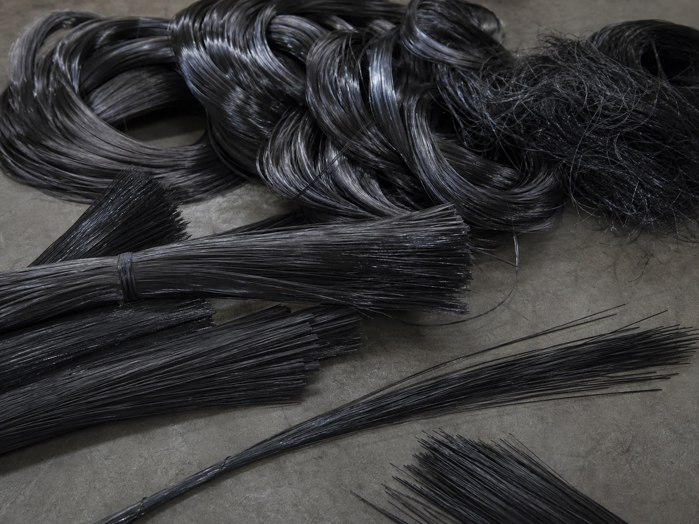
Carbon Fiber
Carbon Fiber is selected from its stiffness, recovery, wear, wet-service, chemical, and temperature behavior.
Compare material considerationsCustom Manufacturing RFQ
Discuss This Application
Share the working surface, residue, dimensions, material direction, interface, quantity and drawing or sample photo.
Custom Brush RFQ
Request a Custom Cleaning Brush Quote
Upload a drawing, product photo, or sample photo and provide the core dimensions and cleaning conditions.