Custom Cleaning Brush
Cleaning Brush Wafer
Cleaning Brush Wafer provides controlled brush contact for precision electronics and static-control cleaning across contacts, slots, and boards. Working width, brush geometry, mounting, and fill are set around the machine path and the way lint, oxide, and flux residue must be released or carried away.
Product Features
Fine PBT bristles remove particles from wafer and carrier surfaces — The nonmetallic working face provides controlled contact during cleaning.
Low water absorption helps maintain consistent stiffness — PBT retains its brushing behavior during repeated wet-processing cycles.
Uniform face contact limits local pressure peaks — The brush geometry can be arranged to clean across the active wafer area with even engagement.
Wet-process construction supports rinsing — The head can operate with DI water or the specified cleaning liquid when compatible materials are confirmed.
Machine interface is matched to the cleaning tool — Core, holder, and drive details are produced from the equipment drawing rather than assumed.
Configured to the wafer process — Working diameter or width, PBT filament size, trim, density, core, mounting, and cleanliness requirements can be customized.
Product Overview
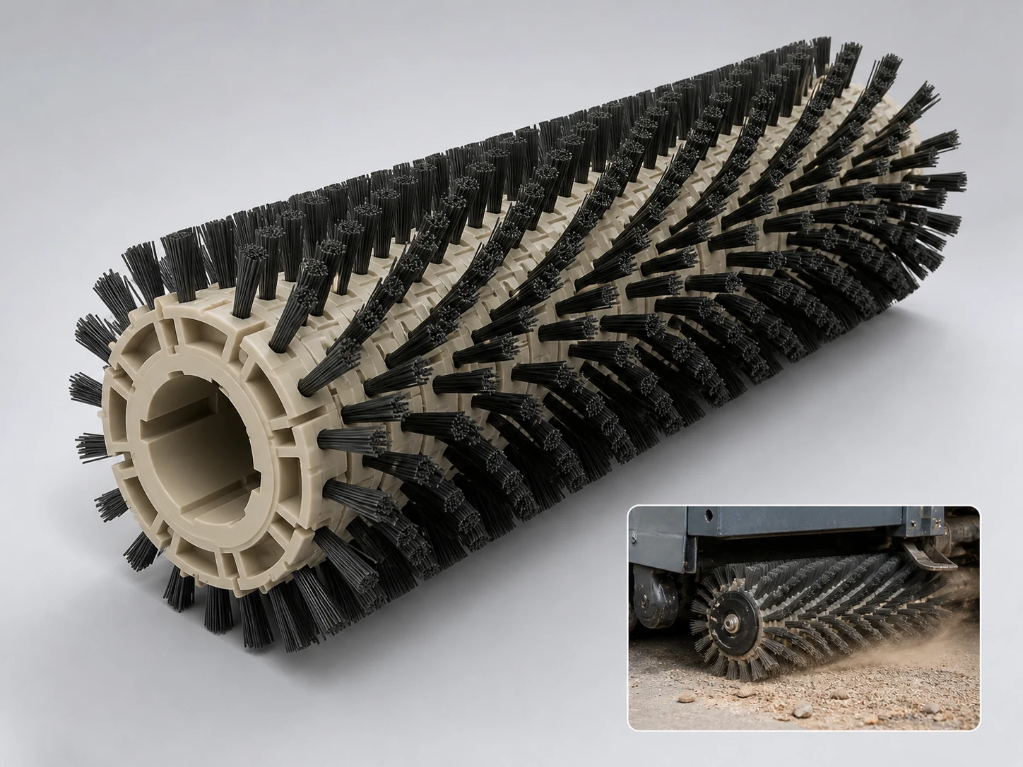
Cleaning Brush Wafer is used where repeatable contact is needed across contacts, slots, and boards rather than isolated hand cleaning. The active brush face clears lint, oxide, and flux residue while the holder, shaft, plate, or hub stays outside the interference path and supports the required working width. The brush must control contact load, particle shedding, conductivity, and access to fine features.
Key dimensions start with Brush head diameter 80–250 mm and Brush head length 100–500 mm. This product uses a roller or conveyor-brush structure for continuous contact across a moving or wide surface. The specified interface is shaft-mounted / flange. PBT are the principal material directions in the current specification. For machine-driven use, confirm the shaft or hub, available clearance, rotation direction, and customer-supplied speed.
Technical Specifications
| Working width | 100–500 mm |
|---|---|
| Brush diameter | 80–250 mm |
| Core or shaft | 20–100 mm |
| Pore or abrasive grade | PVA pore grade or 36–400 abrasive grade |
| Runout | ≤0.2 mm for precision roller assemblies |
| Contact setting | Use 0.5–3 mm engagement or a surface load below 2 N/cm² on fragile substrates. |
| ESD resistance | 10³–10⁹ ohms where required |
| Surface load | 0.5–3 N/cm² for controlled low-pressure contact |
| Fill materials | PBT |
| Cleaning zone | precision electronics and static-control cleaning |
| Contact surface | contacts, slots, boards, terminals, optical end faces, films, carriers, and precision housings |
| Residue class | lint, oxide, flux residue, polishing particles |
| Access and motion | the brush must control contact load, particle shedding, conductivity, and access to fine features |
| Cleaning duty | precision electronics, static-control cleaning on contacts, slots, boards, terminals |
| Variant configuration | Cleaning Brush Wafer: wafer construction with PBT fill for precision electronics and static-control cleaning on contacts, slots, boards, terminals. |
Application Areas
Cleaning Brush Wafer is primarily mapped to Semiconductor Wafer & Chip Cleaning. Before changing the application, review the contact surface, debris removal path, and acceptable surface condition.
- Cleaning Brush Wafer is best suited to wafer, semiconductor, CMP pad, silicon, and precision-substrate cleaning or polishing.
- The antistatic, conductive, PVA, abrasive, plate, disc, or precision roller brush follows wafer face, CMP pad, carrier, precision surface, chamber component, and process roller while the fill displaces slurry, particles, polishing residue, oxide, film, and clean-process contamination.
- Use this configuration when the available access supports low-load contact on electronics, connectors, PCB, battery, ceramic, or semiconductor surfaces.
Selection Guidance
Structure fit
Match the roller and conveyor brush geometry to contacts, slots, and boards, the available access, and powered operation. Confirm Brush head diameter 80–250 mm and Brush head length 100–500 mm against the complete working envelope before finalizing the brush.
Contact material
Choose from PBT according to the behavior of lint, oxide, and flux residue, the surface sensitivity, and any wet, chemical, temperature, or hygiene requirements. Stiffness is not decided by the material name alone. Filament diameter, free trim length, and density also matter.
When to use another solution
For Cleaning Brush Wafer, use another cleaning method when lint, oxide, and flux residue cannot be released by controlled filament contact, when contacts, slots, and boards cannot tolerate the selected contact material, or when the access path prevents safe engagement and residue removal.
Customization Options
| Brush Head Diameter (mm) | 80–250 |
|---|---|
| Brush Head Length (mm) | 100–500 |
| Handle Length (mm) | Not Applicable (No separate handle in this product configuration) |
| Handle Grip Diameter (mm) | Not Applicable (No explicit grip or handle-diameter dimension in the product specification) |
| Bristle Material | PBT |
| Handle Material | 304 Stainless Steel |
| Mounting / Interface | Shaft-Mounted / Flange |
| Grip Style | Not Applicable (Machine-Mounted Brush) |
| Color | Custom PANTONE Color ([Industry Reference Range]) |
| Logo Process | Laser Engraving / Screen Printing / Pad Printing ([Industry Reference Range]) |
| Surface Treatment | Smooth / Textured / Overmolded / Coated (Depending on Substrate; [Industry Reference Range]) |
Frequently Asked Questions
How should Cleaning Brush Wafer be selected?
Start with wafer, semiconductor, CMP pad, silicon, and precision-substrate cleaning or polishing, wafer face, CMP pad, carrier, precision surface, chamber component, and process roller, and slurry, particles, polishing residue, oxide, film, and clean-process contamination. Then set Working width, Brush diameter, and Core or shaft, choose the fill from the material and residue table, and match the mounting interface and operating condition.
Which dimensions define Cleaning Brush Wafer?
The primary dimensions are Working width (100–500 mm), Brush diameter (80–250 mm), and Core or shaft (20–100 mm). Also provide the minimum clearance, working envelope, trim or engagement, and the existing holder, shaft, stem, thread, or handle.
Which filament or contact material is used for Cleaning Brush Wafer?
The primary options are PBT. The final choice follows surface sensitivity, residue adhesion, wet or dry use, temperature, chemicals, conductivity, and required cutting action.
When is Cleaning Brush Wafer not the best cleaning method?
Cleaning Brush Wafer is not the first choice for ionized air, vacuum, PVA sponge, megasonic, wipe, or solvent cleaning where bristle contact is unsuitable.
What information is required to quote Cleaning Brush Wafer?
Send the part or machine drawing, photos of wafer face, CMP pad, carrier, precision surface, chamber component, and process roller, Working width, Brush diameter, Core or shaft, and Pore or abrasive grade, the residue description, wet or dry conditions, motion or use method, temperature, preferred PBT, quantity, and the existing interface or sample.
RELATED BRUSH RESOURCES
Recommended Reading & Related Brush Resources
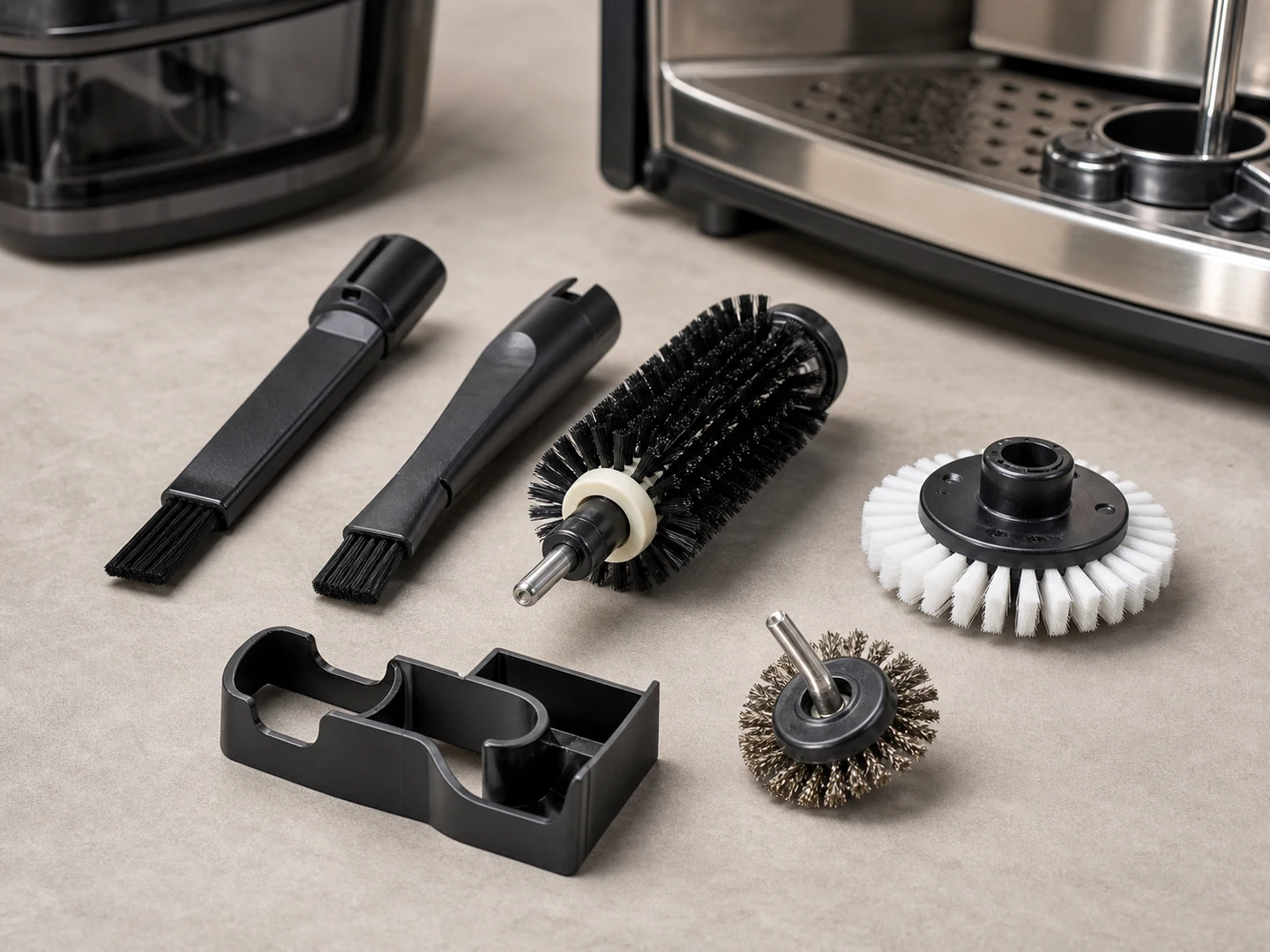
Custom Roller and Conveyor Brushes
Choose a roller or conveyor brush when a cylindrical brush must clean, wipe, guide,…
Explore this brush type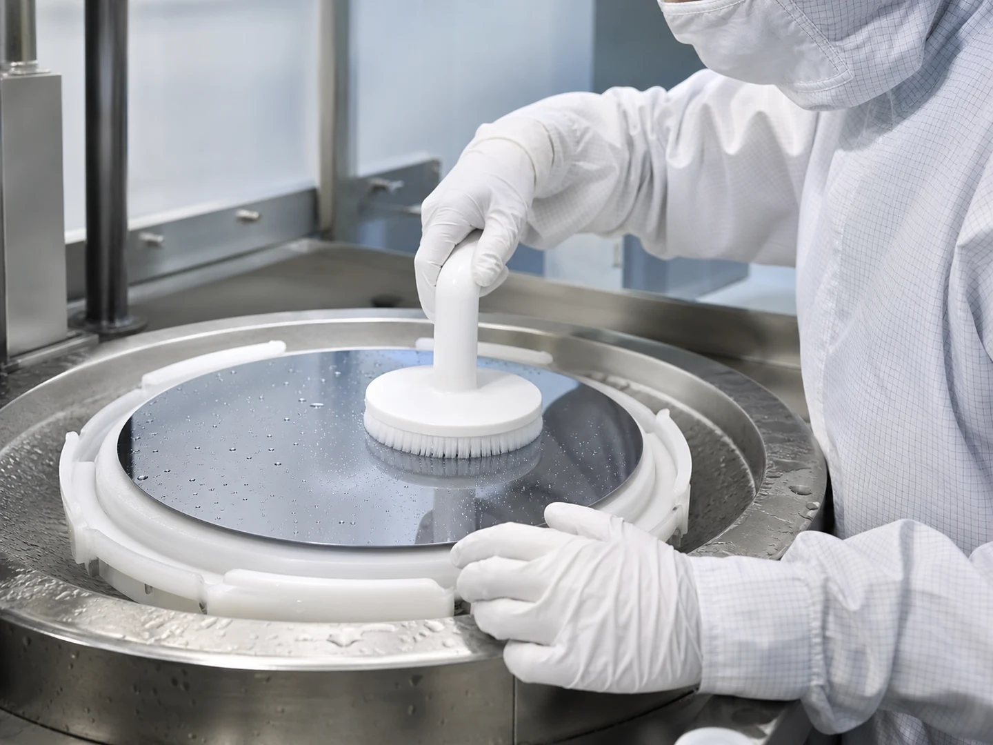
Semiconductor Wafer & Chip Cleaning
For Semiconductor Wafer & Chip Cleaning, the brush must reach the working area, disturb…
Review application guidance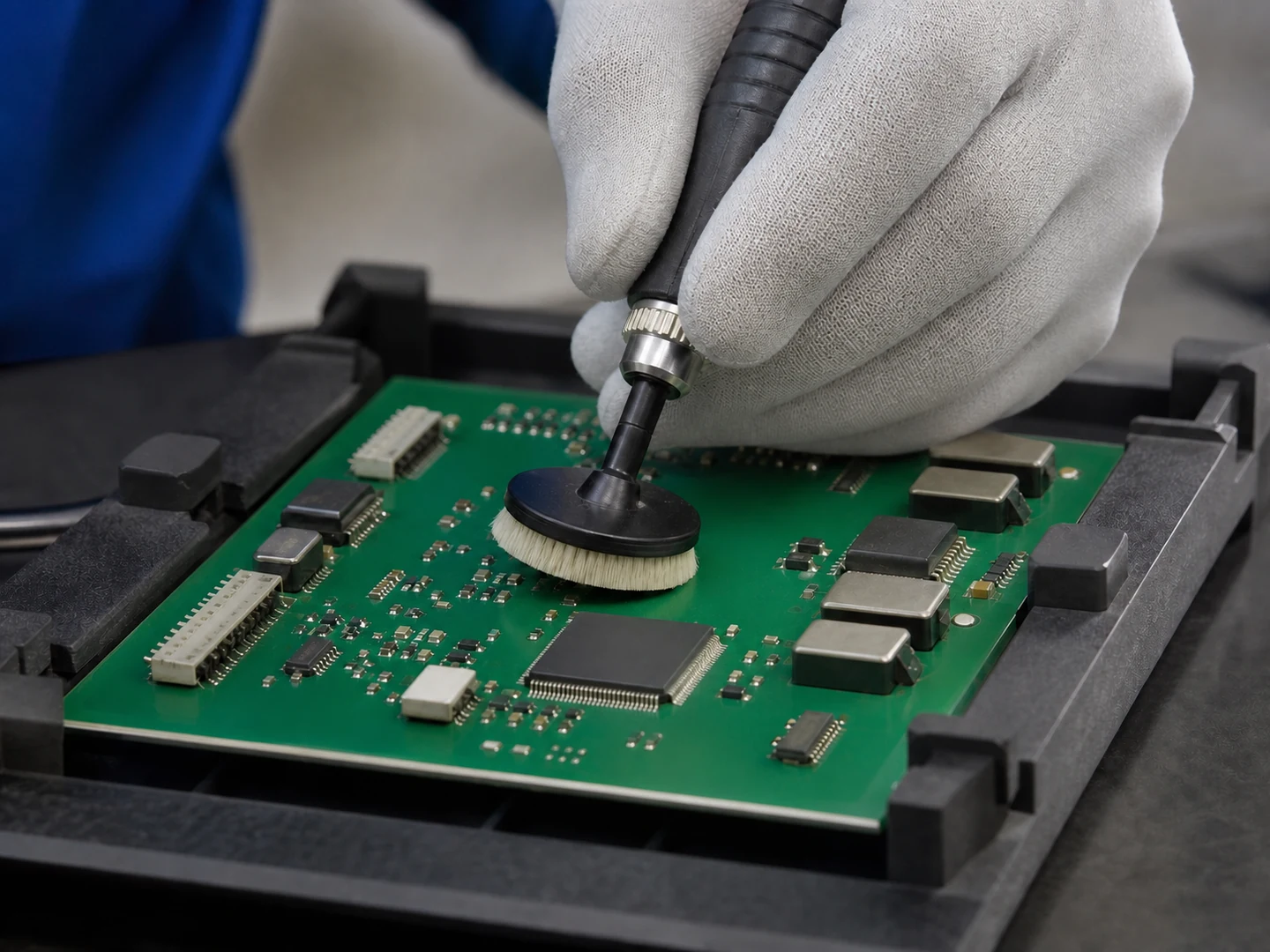
PCB Cleaning
For PCB Cleaning, the brush must reach the working area, disturb or collect flux/weld…
Review application guidance
PBT
PBT is selected from its stiffness, recovery, wear, wet-service, chemical, and temperature behavior. Do…
Compare material considerationsCustom Manufacturing RFQ
Upload the Brush Drawing, Product Photo or Sample Details
Send the key measurements, cleaning requirement, residue, material direction, mounting method, quantity, and drawing or photo.
Custom Brush RFQ
Send Your Brush Project
Upload a drawing, product photo, or sample photo and provide the core dimensions and cleaning conditions.