What Is a Precision Wafer Brush?
A precision wafer brush is a specifically designed brush used for contact cleaning of semiconductor wafers, substrates, or related sensitive components. Its primary function is to remove loose contamination without scratching the surface, generating additional particles, or leaving chemical residues. Unlike general cleaning brushes, precision wafer brushes are manufactured in cleanroom-compatible environments, undergo rigorous cleaning and packaging processes, and are often tested for low particle release, low outgassing, and surface resistivity control.
In cleanroom-adjacent work—such as wafer dicing, die attach, wire bonding, PCB inspection, and optical assembly—operators need a brush that can effectively dislodge dust or flux residues while remaining chemically compatible with surrounding processes. The right brush can directly influence yield, equipment uptime, and the frequency of re-cleaning steps.
Common Brush Materials and Their Trade-offs
Selecting the right bristle material is the single most important specification. Each material balances particle generation, chemical resistance, temperature tolerance, static dissipation, and cost differently. The table below summarizes the typical options for cleanroom-adjacent applications.
| Material | Key Properties | Typical Use Case | Limitations |
|---|---|---|---|
| Nylon 6.6 | Good stiffness, moderate chemical resistance, low cost | General debris removal on non-critical surfaces | Generates triboelectric charge; not recommended for static-sensitive work without treatment |
| Anti-Static Nylon | Conductive carbon-filled nylon, dissipates static | ESD-safe cleaning of wafers, PCBs, and components in assembly areas | Slightly higher cost; carbon may mark surfaces if binder fails |
| PBT (Polybutylene Terephthalate) | Low moisture absorption, good chemical resistance, low particle shedding | Wet cleaning with solvents, cleanroom wipe-down | Softer than nylon; less effective for baked-on residues |
| PTFE (Teflon®) | Excellent chemical resistance, high purity, low friction | Sensitive surfaces exposed to aggressive chemicals | Expensive; bristles are soft and may not scrub effectively |
| Horsehair | Soft, natural, historically used for delicate surfaces | Final touch-up on optics or polished metals | Organic material; potential for protein residues and microbial growth; not recommended for high-purity semiconductor work |
| Conductive Acrylic Fiber | Static-dissipative, consistent resistivity, cleanroom-washable | Class 1000 or cleaner environments requiring precise static control | Limited availability; higher material cost |
How Size, Diameter, and Bristle Stiffness Affect Performance
The physical dimensions and stiffness of a wafer brush determine cleaning efficiency, risk of surface damage, and operator fatigue. Three variables matter most:
- Bristle diameter: Common sizes range from 0.05 mm to 0.2 mm. Finer bristles (≤0.1 mm) conform better to surface topography and reduce scratch risk but may lack the stiffness to dislodge adhered contamination. Coarser bristles clean faster but can mar soft films.
- Overall brush length and row width: Brushes for manual wafer cleaning typically have a head length of 10 mm to 50 mm with 3–10 rows of bristles. For automated wafer scrubbers, dimensions must match the equipment fixture exactly—often requiring custom brackets.
- Stiffness: Often a function of material and bristle length. A shorter trim length gives a stiffer brush. For cleaning between wafer fine pitch interconnects, a stiff, short-trimmed brush may be needed; for final surface dusting, a long, soft brush is safer.
Handle, Core, and Mounting Options
Precision wafer brushes are not universal consumables. The way the brush is held or mounted influences operator comfort, cleaning repeatability, and compatibility with automated equipment.
- Plastic handles: Lightweight, can be anti-static. Common for manual wafer inspection stations.
- Stainless steel cores: Durable, autoclavable, but may introduce particle shedding if not passivated. Often used in wet benches.
- Brush-only inserts (coreless): Designed to clip into proprietary holders; replace only the brush element to reduce waste.
- Threaded or clamp mounts: Used in automated scrubbers and robotic end-effectors. Mismatching the mount type is a common ordering error.
Choosing a Precision Wafer Brush: Key Decision Factors
Use the following checklist to narrow down brush specifications before making an inquiry or requesting a sample:
- Residue type: Is it loose dust, dried slurry residue, flux, or organic film? Residue hardness dictates bristle stiffness required.
- Surface sensitivity: Bare silicon, dielectric films, passivation layers, or AR coatings each have a different scratch threshold.
- Wet or dry cleaning: If chemicals or DI water are used, the brush material must resist swelling, degradation, and particle release.
- Chemical exposure: List all solvents, acids, or bases that may contact the brush. Even brief exposure can cause bristle failure.
- ESD requirements: Surface resistivity target (e.g., <10^6 ohm/square) and the need for conductive/dissipative properties.
- Operating frequency: High-usage brushes may require sturdier construction and a defined replacement schedule.
- Custom dimensions: If the brush must fit a holder, provide a drawing with tolerances. Standard catalog sizes rarely fit retrofit equipment perfectly.
- Cleanroom packaging: Confirm if double-bagging, vacuum-sealed, or cleanroom-laundered packaging is needed.
Common Mistakes When Specifying a Wafer Brush
Avoid these frequent errors that lead to re-cleaning, scrapped product, or unnecessary re-orders:
- Choosing by cost drivers per piece rather than cost per wafer yield: A low-cost brush that sheds particles or scratches surfaces can cost far more in lost yield.
- Ignoring bristle diameter and stiffness interaction: “Soft bristle” means nothing without the diameter specification. Define the exact need.
- Using the same brush for all cleaning steps: A brush that works for post-CMP clean may be too aggressive for final inspection.
- Skipping chemical compatibility testing: Even widely used nylon can become brittle after repeated IPA exposure. Request manufacturer immersion data.
- Overlooking particle generation: Ask for LPC (liquid particle count) test data from the brush supplier. If they cannot provide it, assume the brush is not cleanroom-adjacent.
- Ordering without a trial sample: Surface interaction cannot be predicted from a data sheet alone. Always run a small batch trial with your actual wafer or substrate.
When a Standard Precision Wafer Brush Isn’t Enough
There are clear boundaries where a manual brush cannot solve the cleaning challenge, and other methods or expert review are required:
- Automated scrubbers with controlled pressure and chemistry: For high-volume production, a robot-held PVA brush or megasonic system will provide control that a handheld brush cannot.
- Particle removal below 1 µm: Sub-micron particles often require wet chemical clean, CO2 snow, or laser cleaning.
- Bonded wafer pairs or MEMS devices with fragile structures: Brushing can damage released structures. Non-contact cleaning or gentle spray methods are preferred.
- Process requiring validated cleanroom protocols: If the environment must meet ISO 14644-1 Class 3 or better, the entire brush supply chain must be certified. A standard “cleanroom brush” may not be enough without full documentation.
- Custom fit that falls outside standard tolerances: If your holder is non-standard, a supplier drawing review and custom brush mold are necessary. Off-the-shelf modifications (e.g., trimming bristles) introduce new contamination risks.
Final Takeaway
A precision wafer brush is a small component with an outsized influence on yield in cleanroom-adjacent processes. The correct choice depends on matching bristle material and geometry to the residue type, surface risk, and operating conditions, then verifying performance through sample testing. Avoid treating these brushes as ordinary consumables; instead, treat them as a process parameter. When standard options do not fit—literally or in performance—engage a supplier early with a drawing and a description of your chemical and particle goals.
Frequently Asked Questions
What is the difference between a precision wafer brush and a general ESD brush?
A precision wafer brush is manufactured under stricter contamination controls, often with lower ionic contamination, cleaner packaging, and documented particle count data. General ESD brushes are fine for electronics assembly benches but may not meet wafer-level cleanliness standards.
How do I test if a brush leaves residues on my wafer?
Use a witness test: wipe a clean bare silicon wafer with the brush using your typical cleaning motion, then inspect under a collimated light or scanning surface inspection tool for streaks, fibers, or particles. For chemical residues, follow with DI water break test or FTIR analysis.
What bristle diameter is safest for bare silicon wafers?
For bare silicon, a bristle diameter of 0.06–0.10 mm in a soft material like PBT or anti-static nylon is typical. Finer bristles reduce scratch risk but may not remove adhered slurry. Always begin with the smallest diameter that meets removal efficiency, as determined by a sample test.
Can I use a precision wafer brush with acetone or other strong solvents?
Only if the brush material is verified for that solvent. PTFE is compatible with most solvents, but nylon and PBT can degrade. Request a chemical resistance chart from the manufacturer and test in your process before committing to a full lot.
Is horsehair acceptable in cleanroom-adjacent applications?
Generally no. Horsehair is an organic material that can shed protein particles and may support microbial growth. For semiconductor or optics work where yield depends on particle control, synthetic cleanroom-grade materials are strongly preferred.
How often should precision wafer brushes be replaced?
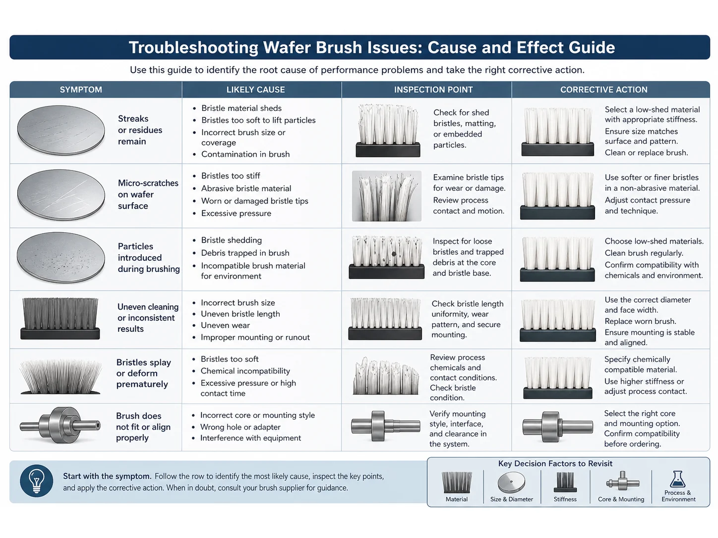
Replacement frequency depends on usage intensity, chemical exposure, and visual inspection. In a manual wafer handling area, a brush might last one shift or several weeks. Establish a maximum number of wipes or a time-based change interval, and monitor for bristle splaying, discoloration, or increased particle counts.
Can a precision wafer brush be autoclaved?
Some can, but not all. Brushes with stainless steel handles and certain synthetic bristles (e.g., PBT, some nylons) may tolerate autoclaving. However, repeated autoclaving can alter bristle stiffness and surface. Confirm with the supplier and consider whether chemical sterilization is an alternative.
What custom dimensions are typically available when ordering a precision wafer brush?
Many suppliers offer custom bristle trim length, overall row length, handle shape, and mounting configuration as long as minimum order quantities are met. Provide a dimensioned drawing that includes tolerances, and specify the required bristle material and packaging. Prototyping may take a few weeks.
Technical References
- EOS/ESD Association — ESD Fundamentals
- EOS/ESD Association — Principles of ESD Control
- NISTIR 4653 — Metrology for the Semiconductor Industry
- ISO 14644-1 Cleanrooms and Associated Controlled Environments
- NIST — Metric SI
Which bristle material fits this job — Nylon PA, PBT or Horsehair?
| Material | Continuous temperature (°C) | Peak temperature (°C) | Water absorption | Hardness |
|---|---|---|---|---|
| Nylon PA | 93 | 121 | 0.3–9% by PA grade and conditioning | Medium to firm; filament diameter and trim length control bending force. |
| PBT | 120–140 | 160–180 | 0.05–0.20% | Shore D 80–90 |
| Horsehair | 60–80 | 100–120 | 8–15% | — |
| AISI 304 Stainless Steel Wire | 400 | 500 | 0% | Rockwell B 70–95 depending on temper and cold work |
| PVA Sponge | 60 | 90 | — | Soft absorbent contact material; hardness/compression is controlled by foam or sponge density. |
Figures as published by Brushtec / DuPont; Perlon; Alleima. Confirm the exact grade against the supplier datasheet before ordering.
When are Roller and Conveyor Brushes the wrong choice for precision wafer brush?
- Roller and Conveyor Brushes — Use a stationary strip brush for a fixed linear seal or wipe, or another process when rotating line contact interferes with the product or cannot discharge the residue safely.
- Nylon PA — The nylon family spans several grades, so heat, moisture and chemical limits should follow the selected PA resin rather than a generic nylon value.
- PBT — Not for heavy rust removal or high-cutting deburring.
- Horsehair — Not for aggressive scrubbing or wet chemical process cleaning.
What should replace Roller and Conveyor Brushes for precision wafer brush?
- Roller and Conveyor Brushes — Roller and conveyor brushes hold cylindrical line contact across a working width, including helix-wound builds where the filament path is set to move loosened material toward one side; a strip brush holds the same line without rotating, so it seals or wipes but cannot carry residue along the width.
- Nylon PA — Compare Nylon PA with PP, PBT, PET. Change material when wet stiffness, temperature, chemical resistance, conductivity, particle shedding, or surface marking becomes the limiting factor.
- PBT — Compare PBT with Nylon, PP, PET. Change material when wet stiffness, temperature, chemical resistance, conductivity, particle shedding, or surface marking becomes the limiting factor.
- Horsehair — Compare Horsehair with Boar bristle, goat hair, microfiber. Change material when wet stiffness, temperature, chemical resistance, conductivity, particle shedding, or surface marking becomes the limiting factor.