Custom Cleaning Brush
Precision Wafer Brush
Low-load, uniform contact for scratch-sensitive substrates, with width, core, fill and density matched to your wafer size and brush-box geometry.
Medium brush
100 pcs
Minimum order
Worked with two hands or on a pole: chimney, gutter and pond-filter brushes, discs, cups and tank brushes.
Production lead time, once the specification is confirmed
- Up to 100 pcsWithin 7 days
- 101–5,000 pcsWithin 14 days
- 5,001–50,000 pcsWithin 21 days
- Over 50,000 pcsConfirmed with your quotation
Peak season can extend these times; the shipping date is confirmed in writing with your quotation. Sampling and shipping are quoted separately.
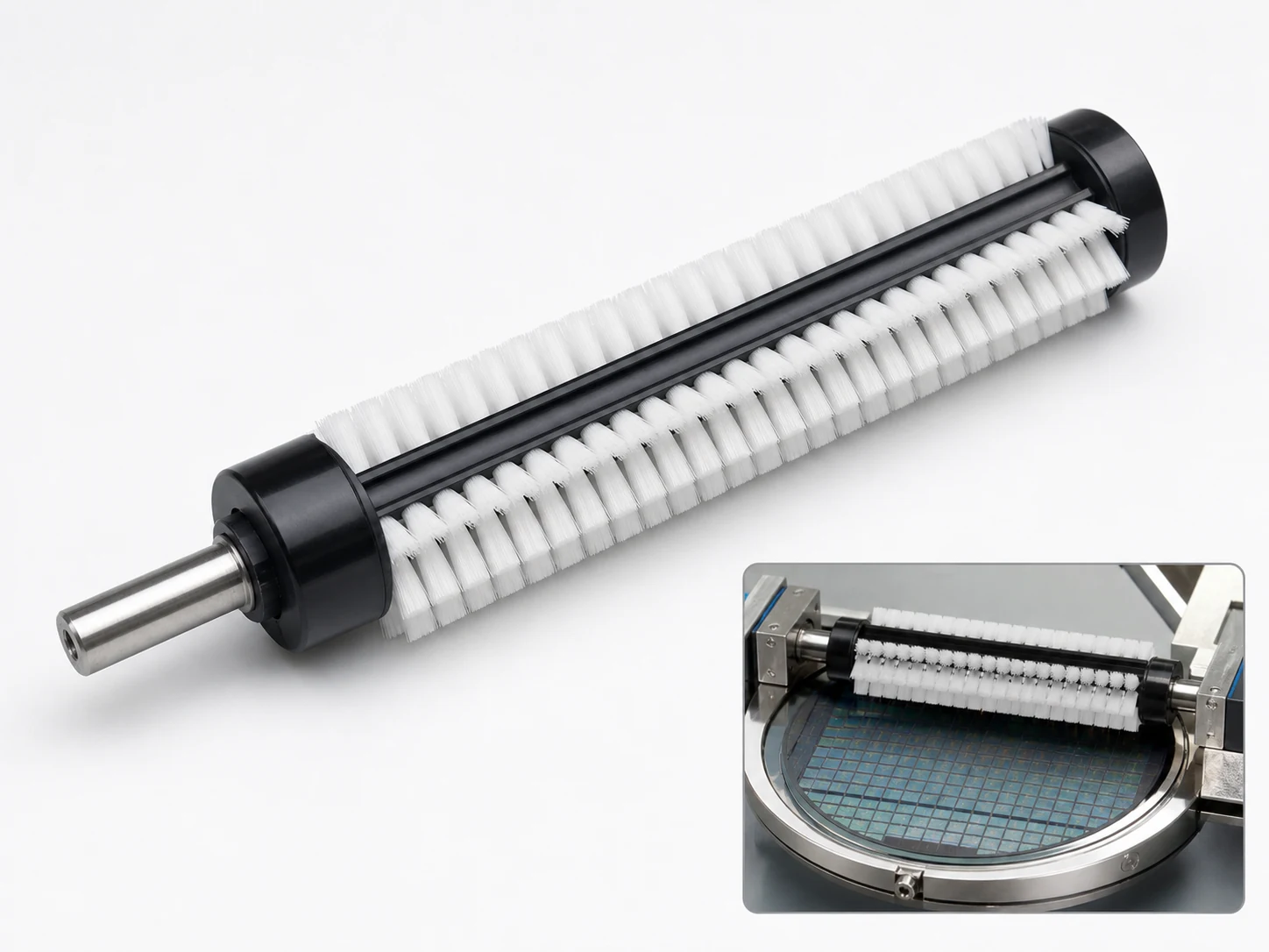
A rotary roller cleaning brush for semiconductor wafer and precision-substrate processing, designed to remove particles, slurry residue, lint, and static-attracted contamination with low-load, scratch-safe contact. Working width, core, filament material, and density are matched to your wafer size, brush-box geometry, and cleaning process.
What can this brush do for you?
Low-load, uniform contact on scratch-sensitive surfaces
The filament and fill configuration is designed to apply low, even pressure across the wafer contact zone instead of concentrated point loads. This reduces the risk of micro-scratches, pattern damage, and film delamination on polished silicon, coated substrates, and other surfaces that cannot tolerate aggressive mechanical scrubbing.
Low particle shedding from the brush itself
Because the brush is made from controlled-density PVA sponge or fine nylon filaments, it does not break down into loose fibers during rotation. This keeps the cleaning tool from becoming a new particle source, which matters when your process is trying to remove particles rather than add them.
Static-attracted dust removal without re-deposition
The brush’s low-contact, conductive-dissipative material options help prevent the triboelectric charging that turns ordinary brush filaments into dust magnets. Combined with a cleaning fluid, the brush lifts particles and carries them away instead of redistributing them across the wafer.
Configurable to your wafer path and brush box
Working width, roller diameter, core diameter, end fittings, and drive interface can all be matched to the wafer diameter and the cleaning module’s holder. The brush engages the full wafer surface on each pass without missing edge zones or overlapping the exclusion area.
Chemical compatibility with typical wafer cleaning chemistries
Fill material is selected for the chemicals in your process: PVA sponge tolerates many aqueous cleaning solutions and holds fluid well, while nylon PA and PBT offer higher mechanical durability and better resistance to certain solvents and alkaline baths. Specify the chemistry so the brush material does not swell, shed, or degrade in service.
What is a Precision Wafer Brush?
A Precision Wafer Brush is a cylindrical rotary cleaning tool used inside semiconductor wafer processing equipment. It is mounted on a drive shaft or core inside a brush box and rotates while the wafer passes beneath it, typically with a cleaning fluid dispensed at the contact zone. The outer working surface—either a molded PVA sponge layer or a dense field of fine nylon/PBT filaments—contacts the wafer with controlled pressure to dislodge contaminants.
This brush is not a hand-held tool. It is an engineered consumable for wafer cleaning modules, post-CMP cleaners, scrubbers, and other automated precision-cleaning platforms. The brush’s job is mechanical contact that loosens particles and residues while the fluid carries them away, followed by rinse and dry stages in the same tool.
The critical operating parameters are contact pressure, rotation speed, filament density, and fluid coverage. The brush must be concentric, balanced, and free of protrusions that could scratch or contact the wafer unevenly. During use, the brush wears gradually—filament tips round, the sponge compresses, and particle-removal efficiency changes—so replacement intervals are managed by particle counts, surface inspection data, and visual wear checks.
Technical Specifications
The values below represent standard production ranges. All dimensions, materials, and interfaces are configurable to the cleaning tool and process.
| Parameter | Value / Options |
|---|---|
| Working width | 100–300 mm, matched to wafer diameter or cleaning path |
| Roller diameter | 20–80 mm, selected for brush engagement depth and module clearance |
| Core diameter | 10–40 mm, matched to drive shaft, mandrel, or end fittings |
| Filament diameter | 0.05–0.30 mm; finer filaments for gentler contact and lower shedding |
| Fill material | PVA sponge (hydrophilic, high fluid retention) or soft nylon PA; PBT available for chemical resistance |
| Contact force | Low-load, uniform distribution appropriate to scratch-sensitive substrates |
| Core material | Stainless steel, aluminum, or polymer depending on chemical and weight requirements |
| End fittings | Custom-machined to match brush holder, drive key, or shaft interface |
| Operating environment | Cleanroom compatible; material grade selected for cleaning chemistry, temperature, and static requirements |
| Dimensional tolerances | Controlled for concentricity and runout to maintain uniform wafer contact |
| Brush type | Custom Roller and Conveyor Brushes |
| How it is driven | Machine-driven, mounted in the equipment |
| Cleaning target | post-cmp, post-dicing and backside, and pre-deposition and pre-lithography cleaning |
| Surface or part | roller, substrates, optical end faces, precision housings, edges, boards, carriers, and glass |
| Residue or debris | particles, lint, slurry, dust, static-attracted dust, static-attracted contamination, flux residue, and polishing residue |
| Mounting / connection | Custom-machined to match brush holder, drive key, or shaft interface |
Where does this brush work best?
- Post-CMP cleaning: removes slurry particles and polishing residue from oxide, metal, and dielectric surfaces after chemical mechanical planarization.
- Post-dicing and backside cleaning: lifts silicon dust and debris from wafer backside or sawn substrates before die attach or packaging.
- Pre-deposition and pre-lithography cleaning: reduces particle-related defects on wafers entering critical process steps.
- Precision substrate cleaning: glass panels, photomasks, optical end faces, films, carriers, and precision housings that need gentle mechanical contact with low contamination risk.
- Static-control cleaning: removes lint, flux residue, and static-attracted dust from boards, terminals, contacts, and component surfaces in electronics assembly where ESD control matters.
How do I choose the right one?
Start with the wafer and equipment, then select the contact material for your residue and process.
Match working width and core to the cleaning module
Measure the brush box opening, the wafer diameter, and the required cleaning coverage. The working width must fully engage the wafer surface while staying clear of the wafer edges and any exclusion zones. Core diameter and end fittings must match the drive shaft and holder; a misfit causes runout, vibration, and non-uniform contact.
Pick the fill material based on residue and chemical exposure
PVA sponge absorbs and releases cleaning fluid well, resists swelling in many aqueous solutions, and applies very gentle contact—good for soft films, fragile structures, and high particle sensitivity. Nylon PA gives firmer mechanical action and longer wear for tougher residues like polishing particles. PBT suits processes with harsher solvents or higher alkalinity. If static dissipation is required, ask for a dissipative grade or additive package.
Select filament diameter for contact intensity
Finer filaments (0.05–0.15 mm) provide gentler, denser contact and lower particle shedding, ideal for controlled low-load cleaning on polished or patterned wafers. Coarser filaments (0.20–0.30 mm) scrub harder and can remove more tenacious residues but increase the risk of scratching and particle generation. Base the decision on surface sensitivity and defect budgets.
Verify chemical and temperature compatibility
List all cleaning fluids, pH range, concentration, and process temperature. PVA sponge may degrade in strong acids or oxidizers; nylon may soften in strong bases; PBT varies by grade. The brush must survive the process without shedding, dissolving, or changing hardness.
When another cleaning method is better
If the wafer has extremely fragile MEMS structures, tall topography, or deeply recessed features, a roller brush may still be too aggressive or unable to reach into the features. In such cases consider non-contact methods such as megasonic, spray, or immersion cleaning. If the residue is heavy organic contamination or thick films, a solvent pre-clean or plasma process may be needed before the brush step. The brush is a mechanical aid, not a total cleaning solution.
Can I customize this brush?
Yes. Every precision wafer brush is built to the cleaning module and process, not pulled from a generic shelf. To define your configuration, provide the wafer size, cleaning tool model and brush holder drawings, drive shaft or mandrel dimensions, cleaning chemistry, contact pressure or rotation speed limits, and surface defect budget. A sample brush or CAD file of the module accelerates the fit check.
We can adjust:
- Working width and roller diameter to match wafer size, brush box opening, and engagement depth
- Core diameter and material (stainless, aluminum, polymer) with custom end fittings, keyways, or drive interfaces
- Fill material — PVA sponge, nylon PA, PBT, or blends, with optional antistatic or conductive additives
- Filament diameter and density to control contact force, fluid retention, and particle-shedding characteristics
- Surface profile — straight, crowned, or segmented working face to match wafer curvature or edge handling
- Color, marking, and identification for process control and inventory tracking
- Cleanroom packaging — single or multi-pack, vacuum-sealed, labeled, and protected from contamination during storage and transport
If your project requires material declarations, certificates of conformance, cleanliness certification, or third-party testing, we can support those requirements as part of the customization process.
When is a precision wafer brush worn out rather than just dirty?
How do I know when to replace the precision wafer brush?
Track particle counts on monitor wafers, surface inspection defect maps, and visual brush condition. If defect counts trend upward, the brush has visible tip rounding or compaction, the PVA surface appears glazed or torn, or the brush no longer rebounds after compression, schedule replacement. Do not wait for particle excursions to reach your limit line.
What should I check before installing a new brush?
Inspect the core for straightness, nicks, corrosion, or end-fitting damage. Confirm the working width and diameter match the module. Check that the brush is clean and free of packaging lint or debris. If the brush has a protective film or conditioning requirement, perform the pre-use break-in or rinse step specified for your process.
Does the brush remove all particles in one pass?
No. The brush loosens and dislodges particles; the cleaning fluid carries them away, and subsequent rinse and dry steps complete the removal. If particles remain after a full brush-and-rinse cycle, adjust contact pressure, fluid flow, or rotation speed, or verify that the brush fill material is still effective for the residue type.
Can I use the same brush with different cleaning chemistries?
Only if the fill material is compatible with all chemistries in the sequence. Changing chemistry mid-life can swell, embrittle, or dissolve the brush and generate particles. Check the material resistance for each fluid, temperature, and concentration. When in doubt, dedicate brushes to specific chemistries or ask us to verify compatibility.
What is the acceptable runout for a wafer brush?
Runout should be low enough that the brush surface contacts the wafer evenly across the full working width. Typical targets are under 0.05 mm TIR, but the actual requirement depends on your contact force and wafer sensitivity. If you see banding, uneven wear, or localized particle removal, check core straightness and holder alignment first.
Will the brush scratch patterned wafers?
It should not if contact force, filament diameter, and rotation speed are properly matched to the pattern density and film stack. Fine filaments and PVA sponge minimize the risk, but any mechanical brush can damage extremely fragile structures. Validate the brush on test wafers with representative patterns before production use, and monitor for scratch-related defects after each change.
Guides that go deeper on this
How to Choose Precision Wafer Brush for Wafer Cleaning
Read this guideGuidePrecision Wafer Brush vs Standard Brushes: Wafer Cleaning
Read this guideGuidePrecision Wafer Brush: Material and Size Near a Cleanroom
Read this guideGuideWhen to Use a Precision Wafer Brush on Wafer Carriers
Read this guideGuideHow to Choose Electronics Cleaning Brush for Wafer Cleaning
Read this guideGuideSpecifying Brush Tolerances for Custom and Precision Work
Read this guideRELATED BRUSH RESOURCES
Recommended Reading & Related Brush Resources
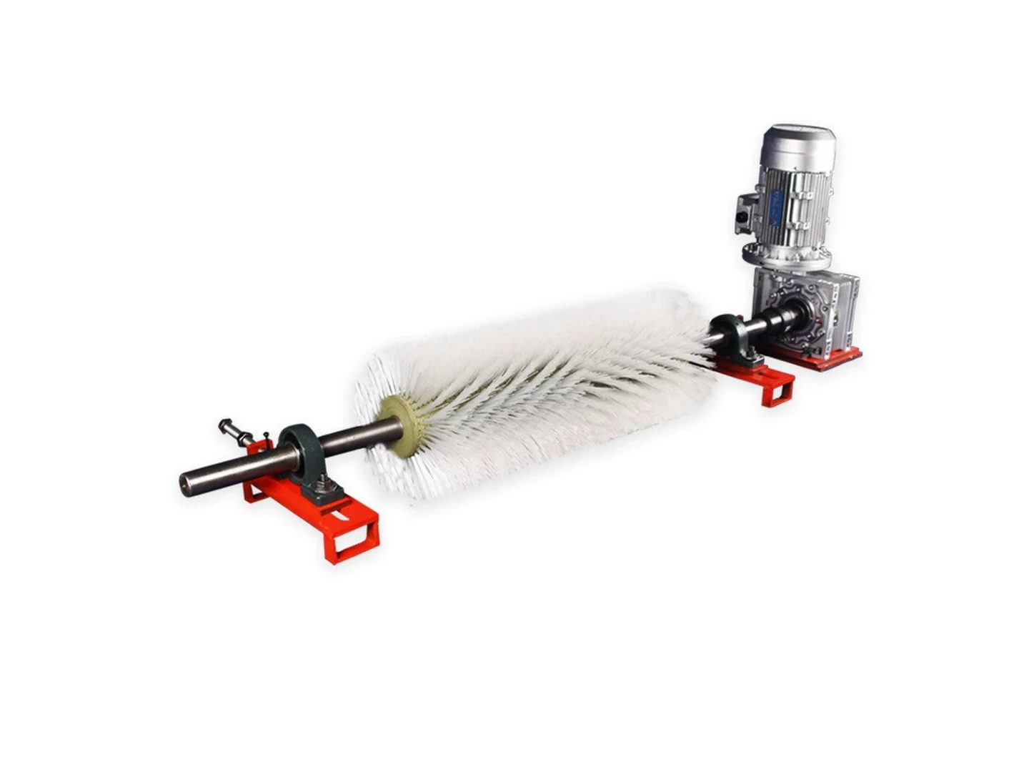
Custom Roller and Conveyor Brushes
Choose a roller or conveyor brush when a cylindrical brush must clean, wipe, guide,…
See how this type is built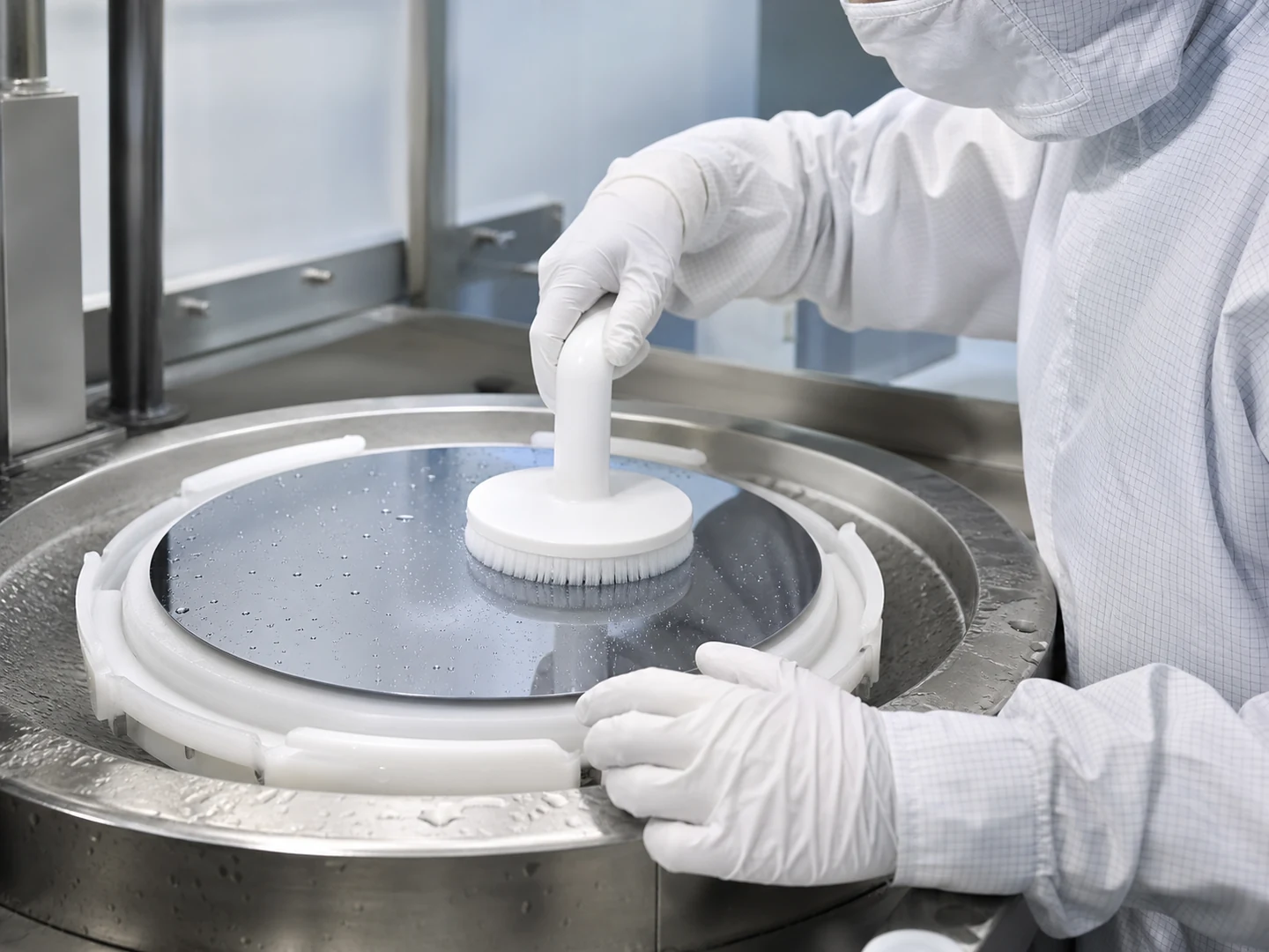
Semiconductor Wafer & Chip Cleaning
For Semiconductor Wafer & Chip Cleaning, the brush must reach the working area, disturb…
See the cleaning job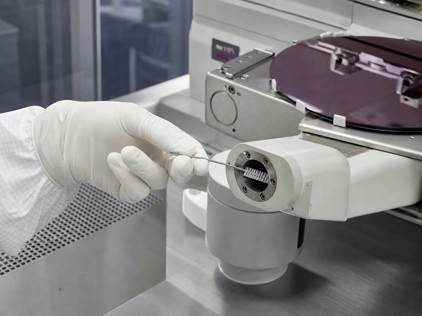
Semiconductor Wafer Handling End-effector Cleaning
For Semiconductor Wafer Handling End-effector Cleaning, the brush must reach the working area, disturb…
See the cleaning job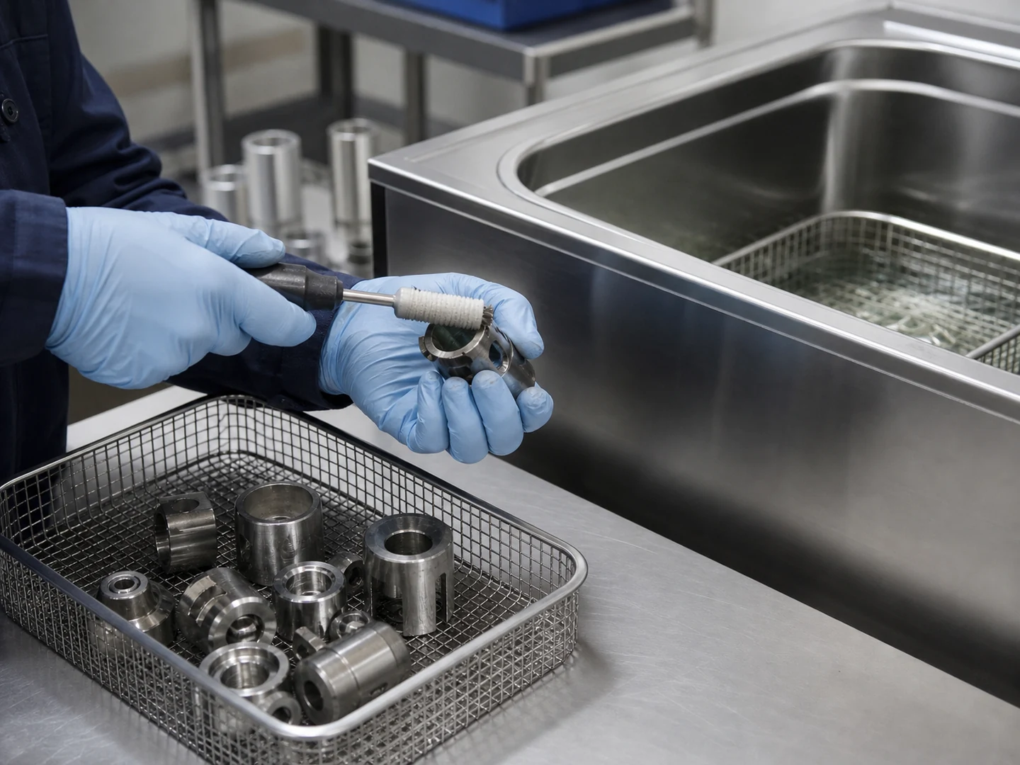
Ultrasonic Cleaning Machine Brush Assistance
For Ultrasonic Cleaning Machine Brush Assistance, the brush must reach the working area, disturb…
See the cleaning job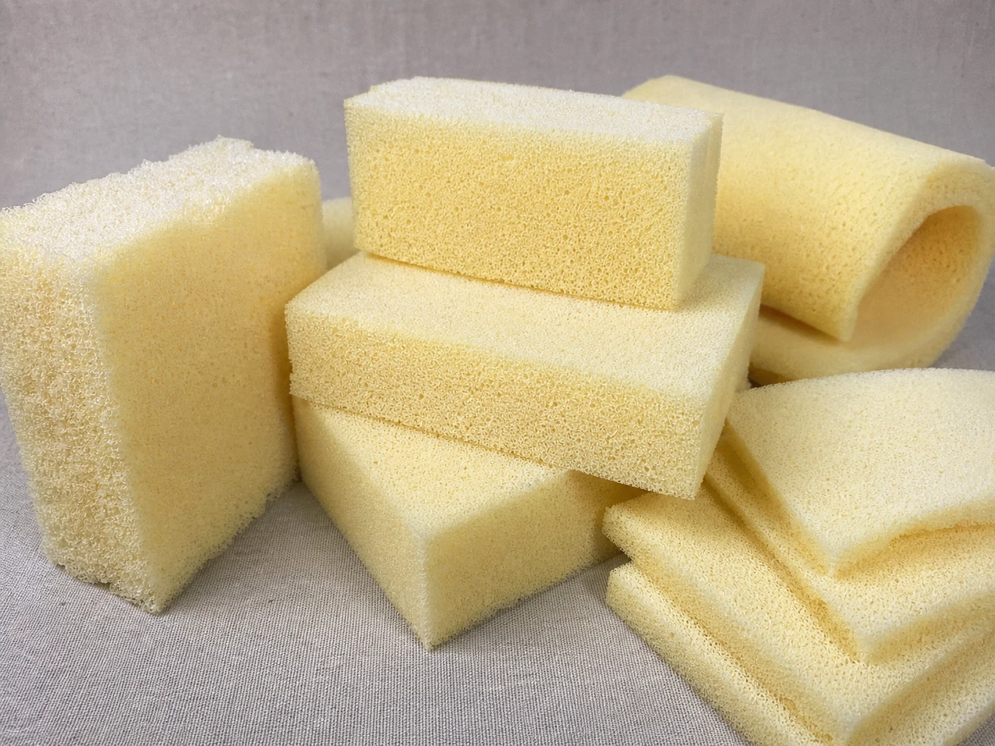
PVA Sponge
Choose PVA Sponge based on its stiffness, recovery, wear, wet-service, chemical, and temperature behavior.
Compare this material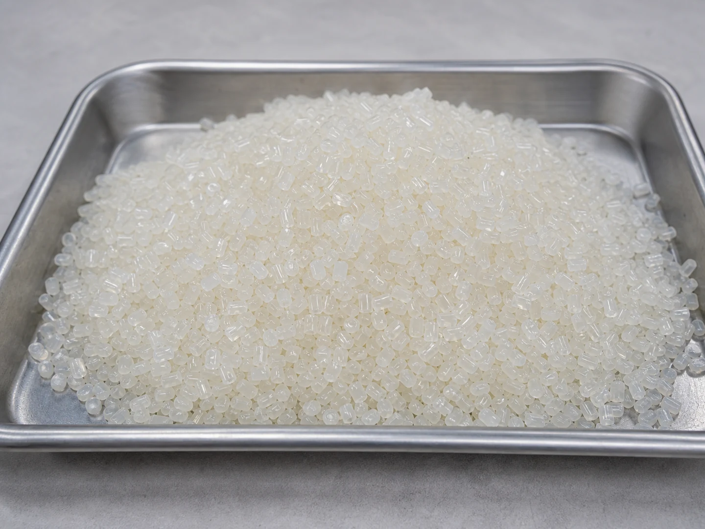
Nylon PA
Choose Nylon PA based on its stiffness, recovery, wear, wet-service, chemical, and temperature behavior.
Compare this material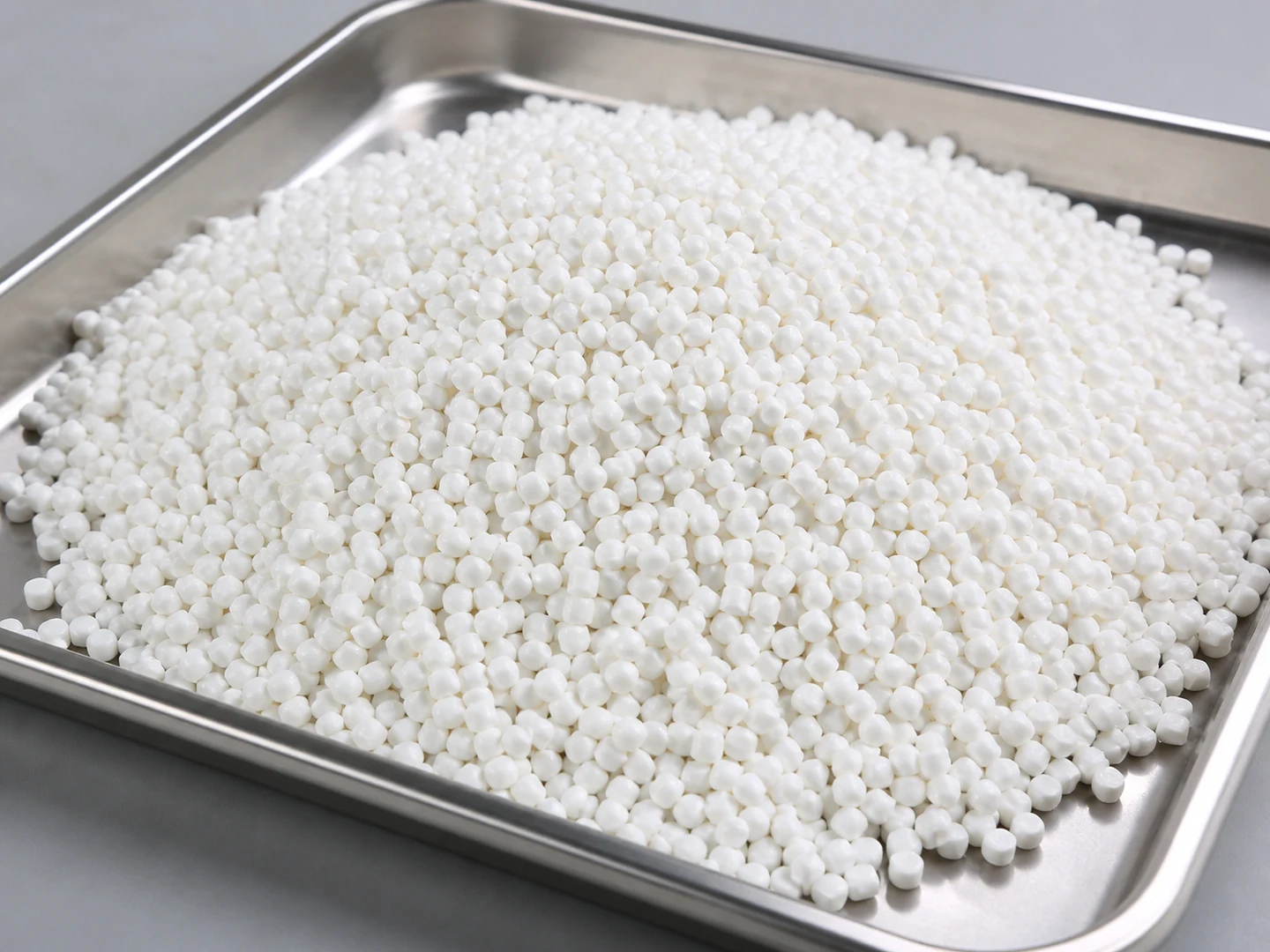
PBT
Choose PBT based on its stiffness, recovery, wear, wet-service, chemical, and temperature behavior. Do…
Compare this material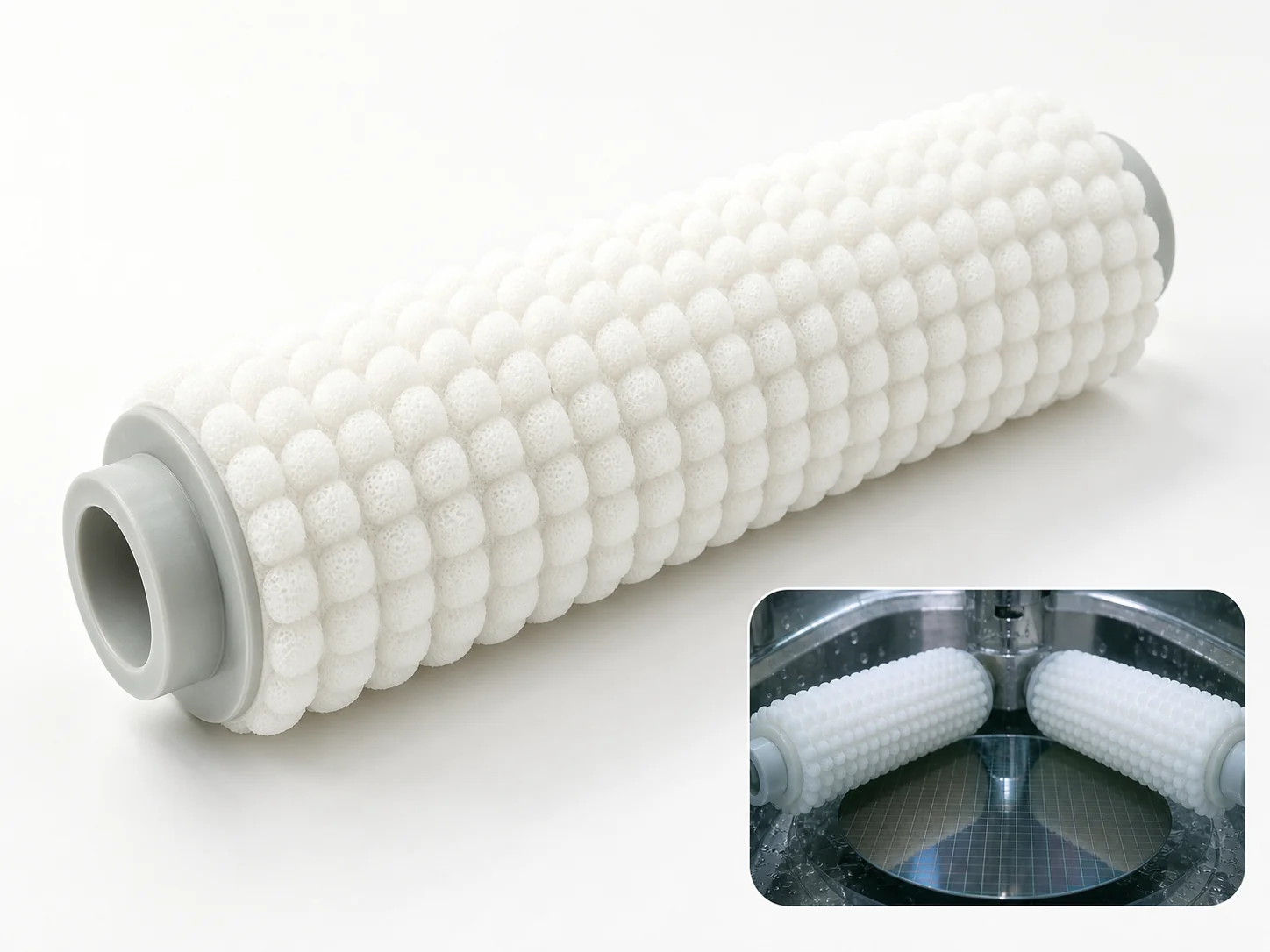
Semiconductor Wafer PVA Cleaning Brush Roller
Tool-matched PVA sponge roller for post-CMP wafer scrubbers. Removes slurry particles without scratching. Custom…
Compare the specificationCustom Manufacturing RFQ
Describe Your Application
To quote this brush accurately, send the size, material, cleaning target, residue, quantity, and any available drawing or sample photo.
Drawing or photo optional — it speeds things up, it does not gate the enquiry.
Custom Brush RFQ
Send Your Brush Project
Upload a drawing, product photo, or sample photo and provide the core dimensions and cleaning conditions.
“We need a brush to remove wet residue from a stainless steel conveyor, about 800mm wide. The current brush wears quickly. We can send photos.”
“We sell drinkware and need a cleaning brush to include with the product. Quantity around 5,000 pieces.”