Application
Semiconductor Wafer & Chip Cleaning
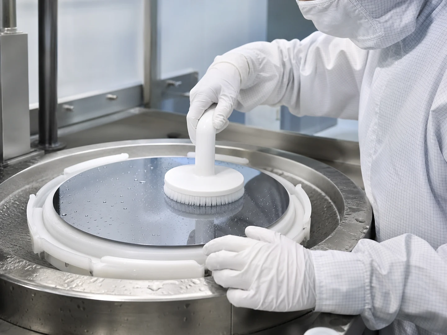
For Semiconductor Wafer & Chip Cleaning, the brush must reach the working area, disturb or collect submicron particles/dust/process residue, and release it without creating unacceptable surface damage or process interference. Brush selection starts with access, contact motion, and the cleaning method used in the process.
At a glance
- Cleaning target
- Submicron Particles/Dust/Process Residue
- Working environment
- Cleanroom
- Cleaning method
- Dry Brushing / Wet Brushing
- Requirements to check
- ISO 14644; Low Ionic Extractables / Low Particle Shedding; ESD Control
At wafer scale a brush is a particle source as much as a particle remover, so PVA sponge, disc and roller brushes are chosen for shedding behaviour and controlled contact before anything else.
What makes Semiconductor Wafer & Chip Cleaning different from other electronics and precision cleaning?
The main difficulty is removing fine dust, oxide, fibers, toner, slurry, and static-charged particles from connectors, slots, PCB, wafers, print paths, and precision components without damaging the surface, loading the brush, or carrying contamination back into the process.
The work happens in cleanroom against submicron particles, dust and process residue.
The part people get wrong: this is not one job. The same equipment carries several targets, each with a different opening and a different residue, and one brush rarely covers them all.
What are the most common cleaning targets in Semiconductor Wafer & Chip Cleaning?
There are 5 distinct targets here, and the brush that suits one will usually not reach another.
| Part or area | Residue type | Cleaning requirement |
|---|---|---|
| Wafer Surface | Submicron Particles, Dust, Process Residue | The face must stay flat against the surface so the whole working width contacts, with filament soft enough not to mark it. |
| FOUP and Cassette | The head must reach the working face and apply even contact without marking the surface. | |
| Process-Chamber Component | The head must enter the cavity and work its inner faces, with a handle long enough to keep the operator clear. | |
| Probe-Card and Test-Fixture | The brush must wrap a projecting part and clean all round it without marking the polished finish. | |
| Wafer Edge and Bevel | The brush must concentrate contact on a small feature without touching the surrounding surface. |
What the equipment leaves you to work inside:
| Parameter | Typical range |
|---|---|
| ESD resistance | 10³–10⁹ ohms where required |
| Trim length | 10–40 mm; 5–40 mm |
| Mounting | Grounded handle, strip, plate, or machine holder; Grounded handle, strip, plate, shaft, or machine holder |
| Carbon or metal fiber diameter | 0.008–0.012 mm |
| Working width / head size | 3–500 mm |
| Contact load | 0.1–2 N/cm² |
Which brush types work for each cleaning target?
Disc, roller, PVA sponge roller, or controlled hand brush matched to machine geometry and wafer or carrier contact.
| Cleaning target | Recommended brush type | Why it fits |
|---|---|---|
| Wafer Surface | Handheld Detail Brushes | A wafer surface tolerates no lateral scratch, so a flat head spreads contact across the face and the cleaning happens in the chemistry, not in the pressure. |
| FOUP and Cassette | A carrier’s slots and rails shed particles onto the wafer edge, so a hand-guided head cleans each slot rather than the outside of the pod. | |
| Process-Chamber Component | Chamber parts are cleaned inside a deep recess, so a head on an extended handle reaches the internal faces where deposition builds. | |
| Probe-Card and Test-Fixture | A probe card is a field of fine needles standing proud, so a soft head is drawn over them in one direction only and never across. | |
| Wafer Edge and Bevel | Roller and Conveyor Brushes | The bevel is a narrow rolled edge that carries residue into every later step, so a small driven brush concentrates on that edge and stays off the face. |
How the brush is usually carried on the machine:
- Driven brush — use when fine dust, oxide, fibers, toner, slurry, and static-charged particles needs repeatable scrubbing or controlled relative movement
- Passive or free-running brush — use for loose contamination and lower process complexity on connectors, slots, PCB, wafers, print paths, and precision components
- Localized hand, strip, or tube brush — use where only an edge, gap, port, or maintenance point needs contact
In practical brush terms: match the construction to the access before anything else. A geometry that cannot reach the target will not be rescued by a better filament.
What filament materials work best for Semiconductor Wafer & Chip Cleaning?
PVA sponge, soft nonwoven or synthetic contact, cleanroom-compatible nylon, and conductive or antistatic filament are considered for particle removal; abrasive mineral is limited to a defined conditioning or polishing step rather than general wafer cleaning.
| If the condition is… | Filament to start with | Why |
|---|---|---|
| Sensitive or coated surface | Nylon PA | balanced flex life and abrasion resistance |
| Wet, washdown, or detergent service | Conductive Nylon | grounded conductive contact |
| Bonded residue or aggressive cleaning | Anti-static Filament | controlled static dissipation |
What the duty rules out before you start comparing grades:
| Constraint | Value for this application |
|---|---|
| Filament hardness | Soft |
| Maximum service temperature | 150°C |
| Chemical exposure | Isopropyl Alcohol; Ultrapure Water; Specified Acid / Alkali Wet-Process Chemicals |
| Cleaning method | Dry Brushing, Wet Brushing |
How do I choose the right brush for my semiconductor wafer & chip equipment?
Shedding and particle data decide the material before contact geometry decides the form; the tool’s own interface then fixes the dimensions.
The order that avoids rework:
- Identify the target part and measure the access opening or clearance
- Describe the residue: what it is, how thick it sits, and how strongly it holds
- Choose the construction that can physically reach that target
- Set the filament from surface risk, working temperature and cleaning chemistry
- Fix filament diameter, free trim length and density for the contact pressure you need
- Run one cycle and check the result before committing to a production quantity
Before you commit to a quantity, send the particle limit, the tool’s contact geometry, and the shedding data your process requires.
When is a semiconductor wafer & chip brush the wrong tool?
Megasonic and wet-bench chemistries remove particles below the size any contact method reliably addresses. Contact is excluded outright on patterned device surfaces and anywhere the process specification forbids it, whatever the brush would otherwise remove.
What common mistakes should I avoid in Semiconductor Wafer & Chip Cleaning?
- Specifying a brush without the particle limit and the shedding data the process actually requires
- Changing brush material while leaving excessive engagement, poor alignment, or no discharge path unchanged
- Copying a worn brush without recording motion, direction, mounting, and the original working diameter
If the brush is already in service and the result is wrong, work from the symptom:
| Symptom | What to change |
|---|---|
| Residue remains | Increase relative motion or discharge, then change filament diameter or density; do not add pressure before checking loading by fine dust, oxide, fibers, toner, slurry, and static-charged particles. |
| Surface marks or scratches | Reduce engagement, use finer or softer fill, and remove trapped abrasive particles from contact with connectors, slots, PCB, wafers, print paths, and precision components. |
| Rapid wear or uneven cleaning | Check alignment, runout, support, motion, temperature, chemical attack, and whether the brush covers the complete working path. |
| Brush loads or redeposits residue | Open the fill pattern or add wash, vacuum, air, scraping, or a collection path so removed fine dust, oxide, fibers, toner, slurry, and static-charged particles leaves the contact zone. |
Questions this page is asked
Which process record should authorize brush contact on a wafer?
Identify the wafer material and layer, completed process step, target residue, approved cleaning tool and the qualified recipe for that product flow. Use a PVA or other brush only where the equipment and process specification explicitly includes it, because post-CMP cleaning does not authorize manual brushing of unrelated wafers or exposed chip structures.
How should a new wafer-cleaning brush lot be qualified?
Condition the brush by the tool procedure and compare representative wafers for particles, scratches, residue removal, wafer-to-wafer uniformity and any required ionic or extractable baseline. Release the lot only when those results and physical checks for dimensions, bonding, pores, shedding and storage condition meet the process limits.
What should release a wafer brush system after maintenance or product change?
Verify the approved chemical and rinse path, brush conditioning state, tool cleanliness, particle baseline and segregation required between product or material families. Confirm the equipment's ESD and electrostatic-attraction controls as a complete verified system before exposed wafers return, rather than relying on a single dissipative component.
Guides that go deeper on this
Continue Exploring
Recommended Reading & Related Brush Resources
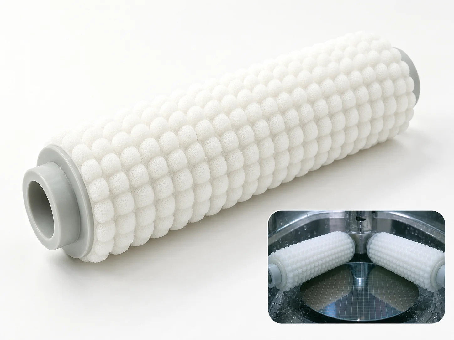
Semiconductor Wafer PVA Cleaning Brush Roller
Tool-matched PVA sponge roller for post-CMP wafer scrubbers. Removes slurry particles without scratching. Custom…
See the specification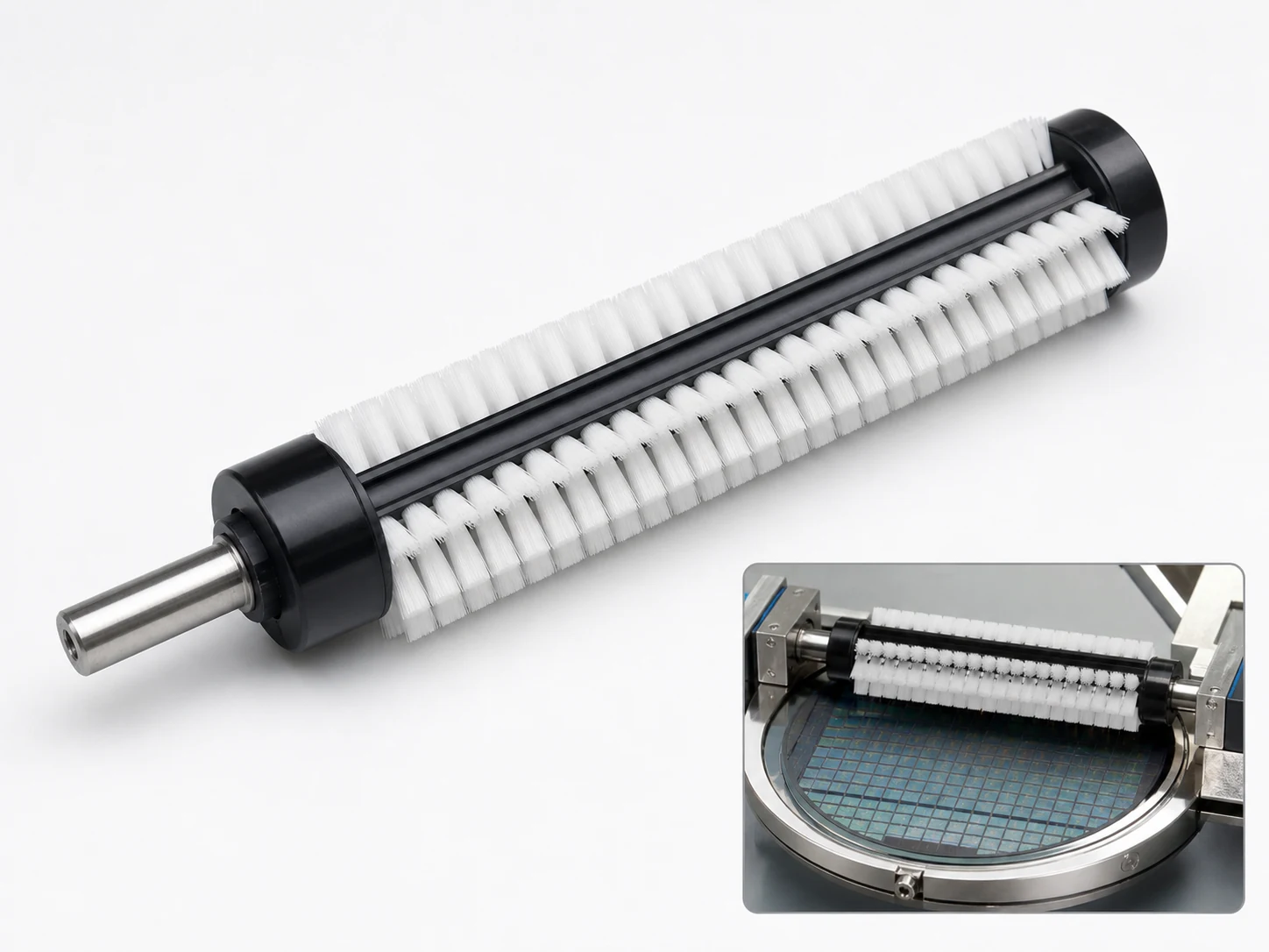
Precision Wafer Brush
Low-load, uniform contact for scratch-sensitive substrates, with width, core, fill and density matched to…
See the specification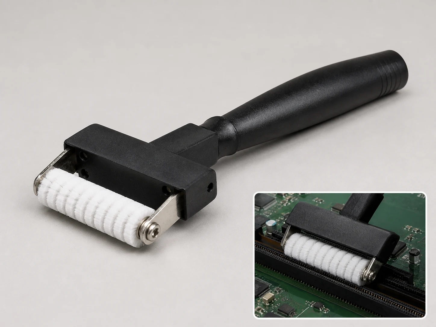
Semiconductor Brush
Custom semiconductor cleaning brushes with PVA sponge or fine nylon fill. Engineered for wafer…
See the specification
Custom Handheld Detail Brushes
Choose a handheld detail brush when you need direct control in seams, recesses, fittings,…
See how this type is built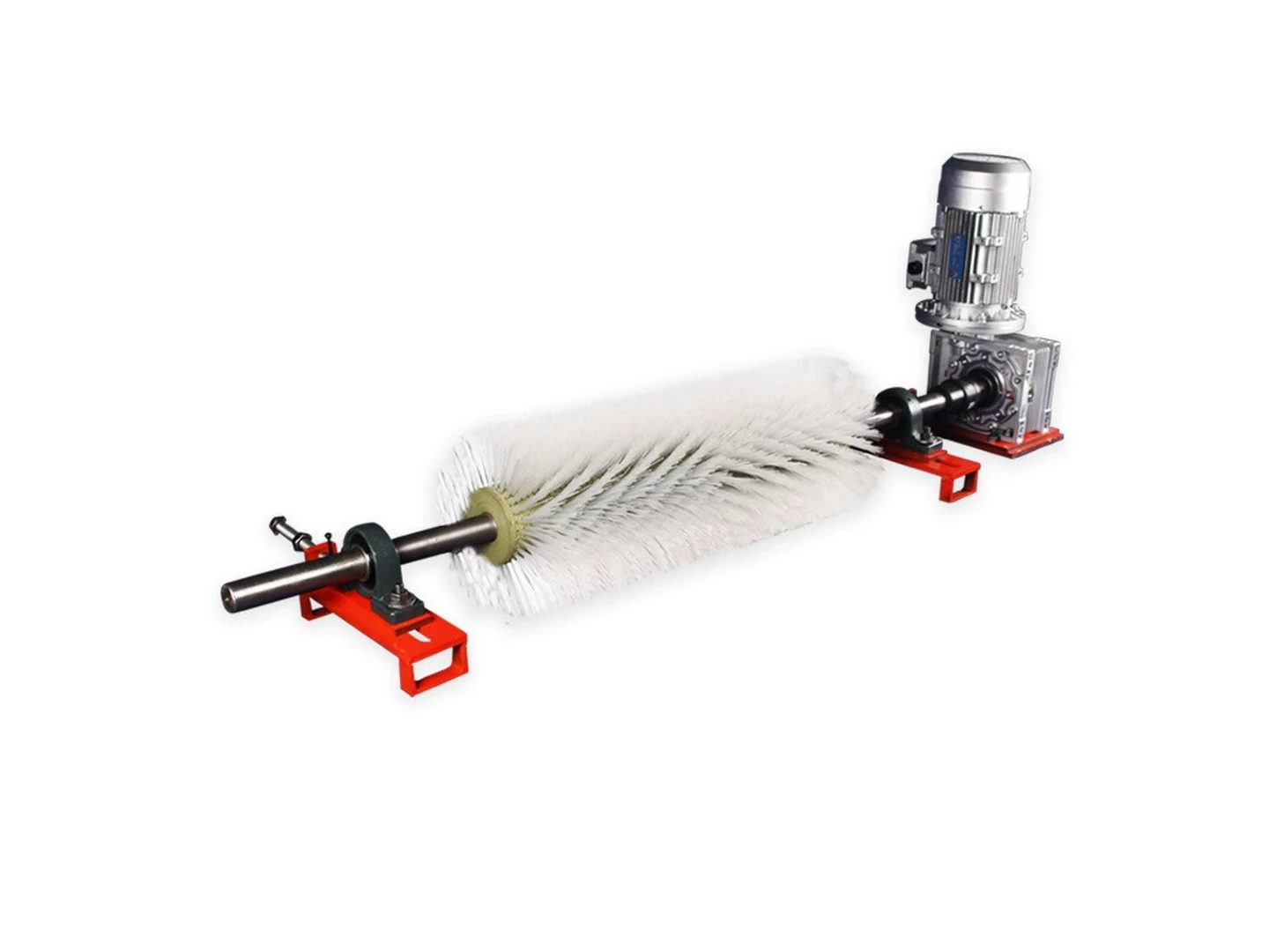
Custom Roller and Conveyor Brushes
Choose a roller or conveyor brush when a cylindrical brush must clean, wipe, guide,…
See how this type is built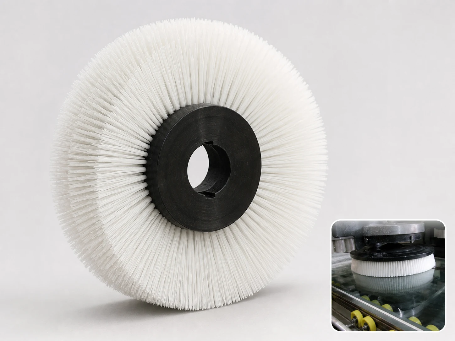
Custom Disc Brushes
Choose a disc brush when a circular face must scrub, wipe, polish, sweep, or…
See how this type is built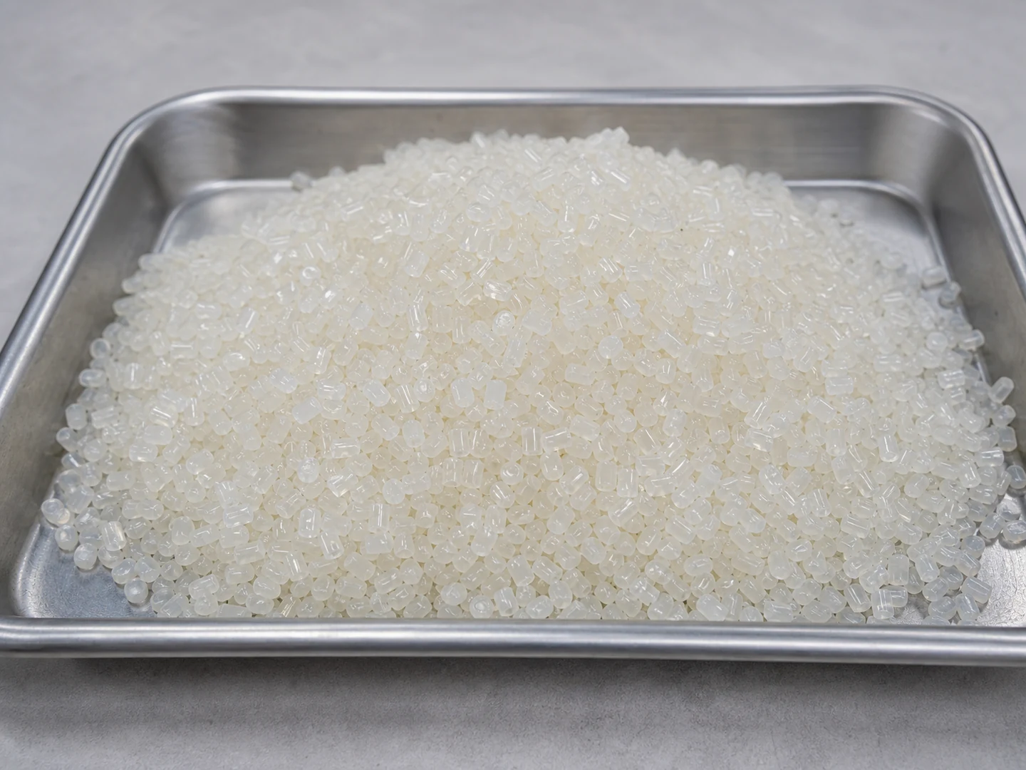
Nylon PA
Choose Nylon PA based on its stiffness, recovery, wear, wet-service, chemical, and temperature behavior.
Compare this material
PBT
Choose PBT based on its stiffness, recovery, wear, wet-service, chemical, and temperature behavior. Do…
Compare this materialCustom Manufacturing RFQ
Discuss This Application
Share the working surface, residue, dimensions, material direction, interface, quantity and drawing or sample photo.
Custom Brush RFQ
Request a Custom Cleaning Brush Quote
Upload a drawing, product photo, or sample photo and provide the core dimensions and cleaning conditions.
“We need a brush to remove wet residue from a stainless steel conveyor, about 800mm wide. The current brush wears quickly. We can send photos.”
“We sell drinkware and need a cleaning brush to include with the product. Quantity around 5,000 pieces.”