Custom Cleaning Brush
Semiconductor Brush
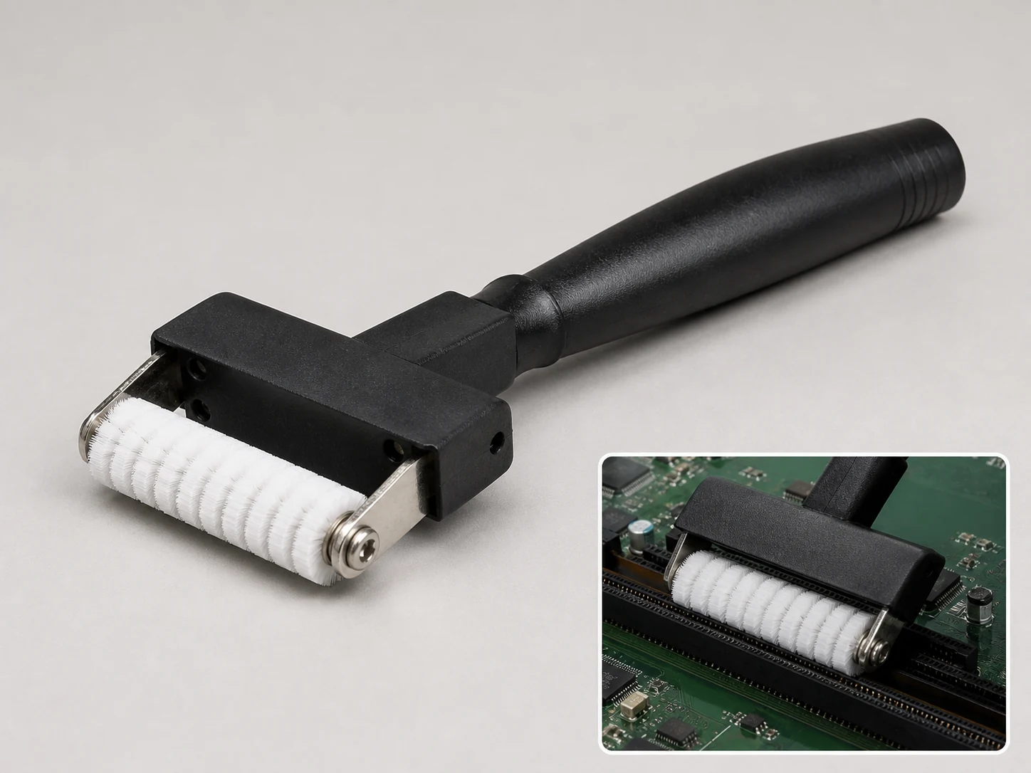
Custom semiconductor cleaning brushes with PVA sponge or fine nylon fill. Engineered for wafer scrubbing, FPD cleaning, and precision part decontamination.
Medium brush
100 pcs
Minimum order
Worked with two hands or on a pole: chimney, gutter and pond-filter brushes, discs, cups and tank brushes.
Production lead time, once the specification is confirmed
- Up to 100 pcsWithin 7 days
- 101–5,000 pcsWithin 14 days
- 5,001–50,000 pcsWithin 21 days
- Over 50,000 pcsConfirmed with your quotation
Peak season can extend these times; the shipping date is confirmed in writing with your quotation. Sampling and shipping are quoted separately.
A precision cleaning brush engineered for semiconductor and microelectronics manufacturing — available in soft PVA sponge or ultra-fine nylon configurations to remove particles, residues, and contamination from wafers, substrates, and critical components without scratching or re-contaminating the surface.
What can this brush do for you?
Removes sub-micron particles without damaging the surface
The PVA sponge’s open-cell structure traps particles within its pores during compression and releases them when DI water flows through, so slurry residue and polishing particles are lifted from the wafer rather than dragged across it. Ultra-fine nylon filaments, as thin as 0.05 mm, reach into slots, contacts, and tight spaces and dislodge debris without leaving scratches on sensitive surfaces.
Keeps contamination out of your process
Every material is selected and processed for low particle shedding and low extractables. The brush itself does not become a source of recontamination. This is critical in semiconductor fabs where a few added particles per wafer can reduce yield.
Applies uniform, low-load contact across the full surface
The cylindrical PVA brush spreads pressure evenly over the wafer or panel, avoiding edge chipping and localized scratching. The porous structure compresses predictably under load, so the cleaning action stays consistent from the center to the edge of the substrate.
Works with your existing wet cleaning chemistries
PVA sponge and fine nylon withstand common aqueous semiconductor cleaning solutions, including SC1, SC2, dilute acids, and DI water. Material grades can be selected for your specific chemical exposure, operating temperature, and rinse conditions.
Prevents ESD damage on electronic components
For boards, contacts, terminals, and other static-sensitive parts, the brush can be supplied with conductive or static-dissipative fill materials and handles. This keeps brushing operations from introducing unwanted electrostatic charge.
Mounts directly to your cleaning equipment
Cores, end fittings, and working lengths are matched to your scrubber, cleaning tool, or manual handle interface. A brush that fits correctly reduces setup time and avoids premature wear from misalignment.
What is a Semiconductor Brush?
A Semiconductor Brush is a cleaning tool built specifically for semiconductor and precision electronics processes. It removes lint, oxide, flux residue, polishing particles, and static-attracted dust from surfaces that cannot tolerate scratches, added particles, or chemical outgassing. The two standard configurations are a cylindrical PVA sponge roller for large flat substrates like wafers and flat-panel displays, and a fine-filament nylon brush for smaller parts, connectors, and enclosures.
In wafer cleaning, the PVA brush is mounted on a rotating shaft and pressed against the wafer surface while cleaning chemistry and DI water are applied. The sponge pores compress and expand as the brush rotates, scrubbing the surface and carrying loosened particles away in the fluid flow. The result is a controlled, low-load mechanical clean that complements chemical action without damaging the wafer.
For precision part cleaning, ultra-fine nylon bristles flex into recesses and contacts, dislodging debris with light pressure. Brush density, filament diameter, and handle or mounting configuration are selected for the specific part geometry and cleaning station.
Operating considerations matter: PVA brushes must be fully hydrated before use, brush pressure and rotation speed should be set within equipment guidelines, and brushes have a finite service life based on particle removal efficiency and physical wear. A properly specified semiconductor brush integrates into the cleaning sequence as a repeatable, low-contamination step.
Technical Specifications
The table below lists standard parameters for semiconductor cleaning brushes. All dimensional and material values can be adjusted to match your equipment and process.
| Parameter | Standard Configuration / Options |
|---|---|
| Brush form | Cylindrical PVA sponge roller or fine-filament precision brush |
| Fill material | PVA sponge (default), ultra-fine nylon 0.05–0.15 mm, or other process-qualified low-shedding media |
| Brush outer diameter | 150–350 mm for wafer scrubbers; smaller diameters for part-level cleaning (custom) |
| Brush length / working width | Matched to wafer path, panel width, or part geometry |
| Core material | 316 stainless steel, titanium, or engineered polymer; custom cores available |
| Porosity (PVA) | 85–95% open-cell structure |
| Hardness / compressibility | PVA sponge soft and highly compressible; nylon filament stiffness selectable per application |
| Operating temperature | Up to 60°C standard; higher-temperature material options available |
| Chemical compatibility | Aqueous cleaning chemistries (SC1, SC2, dilute acids, DI water); solvent compatibility reviewed case-by-case |
| Surface contact | Low-load, uniform contact appropriate for scratch-sensitive substrates |
| ESD options | Conductive or static-dissipative fill and handle available |
| Brush type | Custom Roller and Conveyor Brushes |
| How it is driven | Machine-driven, mounted in the equipment |
| Cleaning target | post-cmp wafer scrubbing, fpd glass, and wafer backside cleaning |
| Surface or part | substrates, panels, connectors, metal, glass, metal surfaces, carriers, and plastic |
| Residue or debris | particles, dust, flux residue, static-attracted dust, lint, oxide, slurry, and fiber |
| Mounting / connection | Shaft-Mounted / Flange |
Where does this brush work best?
- Post-CMP wafer scrubbing: Removes slurry particles and metal contamination from silicon wafers after chemical mechanical planarization.
- FPD glass cleaning: Lifts dust, particles, and residues from flat panel display substrates without scratching the polished surface.
- Wafer backside cleaning: Prepares wafers for bonding, packaging, or inspection by removing particles and films from the non-device side.
- Wafer carriers, cassettes, and FOUPs: Fine nylon brushes remove particles and static-attracted dust from transport components without damaging plastic or metal surfaces.
- Precision housings, contacts, and terminals: Ultra-fine filaments reach into small openings to clean flux residue, oxides, and lint from semiconductor equipment parts.
- Optical end faces and fiber connectors: Soft contact removes debris without scratching polished surfaces.
How do I choose the right one?
Start with the cleaning target and surface material
Identify what you are cleaning: wafer, glass panel, metal contact, plastic carrier, or optical surface. Silicon wafers and glass require non-scratch contact, so PVA sponge or ultra-fine nylon is appropriate. Harder or more tolerant metal surfaces may allow firmer filaments if needed, but most semiconductor applications prioritize low particle generation over aggressive scrubbing.
Select the fill material for the residue and geometry
For flat, large-area substrates, a PVA sponge roller provides the highest particle removal with the lowest scratch risk. For recesses, slots, contacts, and intricate parts, ultra-fine nylon filaments flex into the geometry and dislodge debris. If the part has a mix of flat and intricate surfaces, a custom brush combining different fill types may be required.
Match dimensions and core to your equipment
Measure the brush mounting shaft, the working width needed to cover the substrate, and the space available inside the cleaning chamber. The brush diameter must suit the wafer or panel size and the scrubber’s motion path. Core material and end fittings must be compatible with your cleaning tool, including any dynamic balance requirements.
Consider the chemical environment and temperature
List all cleaning chemistries, concentrations, and temperatures the brush will see. PVA and nylon are generally stable in aqueous solutions, but strong acids, bases, or solvents may require a different material grade or an alternative cleaning method. Provide the full chemical list during specification to avoid premature degradation.
Evaluate ESD requirements
If the brush will contact electronic components, boards, or connectors, specify conductive or static-dissipative materials. Standard PVA and nylon can generate static charge; ESD-safe versions prevent damage to sensitive devices.
When a different cleaning method is more suitable
A semiconductor brush is not the right choice for every residue. Hard ceramic particles embedded in the surface, heavy baked-on films, or photoresist removal typically require chemical stripping, megasonic cleaning, or plasma treatment. The brush complements chemical cleaning by mechanically removing loosely attached particles — it does not replace aggressive chemical or thermal processes. If your residue cannot be removed with light mechanical scrubbing and standard wet chemistry, consider those alternatives first.
Can I customize this brush?
Yes. Semiconductor brushes are always configured to the process, because wafers, panels, and precision parts differ in size, material, and cleaning chemistry. We will need your equipment drawings or mounting specifications, substrate type and size, cleaning chemistry list, operating temperature, desired particle removal target, and any ESD requirements.
We can adjust:
- Fill material and geometry: PVA sponge density, pore size, hardness, and cylindrical profile; nylon filament diameter (0.05–1.2 mm), length, density, and trim pattern; custom low-shedding media options.
- Dimensions: Brush outer diameter, length, working width, and overall profile to match your equipment and wafer path.
- Core and mounting: 316 stainless steel, titanium, or engineered polymer core; custom end fittings, keyways, flanges, or adapter plates.
- ESD options: Conductive or static-dissipative fill, core, or handle materials.
- Color and marking: Custom color for quick identification, laser marking or labeling for lot traceability.
- Packaging: Cleanroom-ready double-bagging, vacuum sealing, individual packaging, or bulk packaging with desiccant as needed.
If your project requires material certifications, particle count data, outgassing test results, or third-party inspection, we can support those requirements during the customization process.
Which filament survives the cleaning and still lasts on a semiconductor brush?
How should I condition a new PVA sponge brush before first use?
Soak the brush in DI water for the time specified in your process documentation, typically 30 minutes to several hours, until the sponge is fully hydrated and has expanded to its working diameter. Then run a dummy wafer or test panel through a cleaning cycle to flush any initial particles from the pores before processing production parts.
How do I verify that the brush is removing particles effectively?
Run a known-particle test wafer or substrate through the cleaning process and measure surface particle counts with a wafer inspection tool (e.g., KLA SP1) before and after brushing. A properly functioning brush should reduce particle counts to the level your process defines as acceptable. Track particle counts over time to monitor brush performance.
When should I replace the semiconductor brush?
Replace the brush when: particle removal efficiency falls below your process limit, the sponge shows visible tears, pore collapse, or permanent deformation, the nylon filaments become bent or matted, or you reach the brush life established during process qualification. Scheduled replacement based on wafer count or hours of use is more reliable than waiting for a cleaning failure.
Can the brush be used with organic solvents?
PVA sponge and nylon have limited compatibility with some organic solvents. Isopropyl alcohol (IPA) is often acceptable for wiping or short-term exposure, but prolonged immersion or aggressive solvents like acetone or NMP can degrade the materials. Provide your full chemical list so we can confirm compatibility or recommend a different media.
Does the brush generate static charge during use?
Standard PVA and nylon can generate static charge when brushing insulating surfaces. If you are cleaning electronic components, boards, or connectors, specify a conductive or static-dissipative version. This reduces the risk of ESD damage and helps prevent re-attraction of dust after cleaning.
What is the difference between PVA and nylon for wafer cleaning?
PVA sponge provides a large, soft contact area ideal for flat wafer surfaces, with high particle removal and low scratch risk. Nylon filaments are better suited to non-planar parts, recesses, and contacts where bristles need to flex into small geometries. For wafer cleaning specifically, PVA is the standard choice; nylon is used for ancillary components and precision housings.
Guides that go deeper on this
Custom Manufacturing RFQ
Describe Your Application
An accurate custom quote starts with the dimensions, working surface, residue, material choice, connection, quantity, and reference files.
Drawing or photo optional — it speeds things up, it does not gate the enquiry.
Custom Brush RFQ
Send Your Brush Project
Upload a drawing, product photo, or sample photo and provide the core dimensions and cleaning conditions.
“We need a brush to remove wet residue from a stainless steel conveyor, about 800mm wide. The current brush wears quickly. We can send photos.”
“We sell drinkware and need a cleaning brush to include with the product. Quantity around 5,000 pieces.”