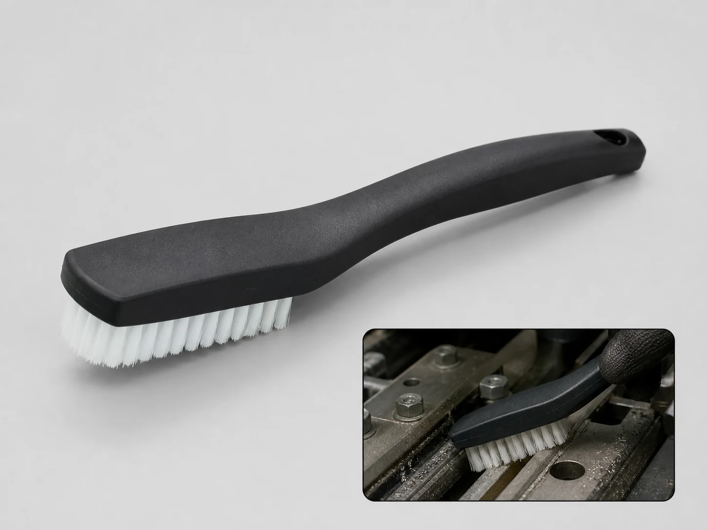
PB33A Brush
PB33A Brush is a 107.95 mm metal-free nylon CMP pad conditioner brush for semiconductor wafer polishing.
- Head Ø
- 80–250 mm
- Head length
- 100–500 mm
Custom Cleaning Brush Manufacturer
PRODUCT CATEGORY
Semiconductor and wafer cleaning puts particle control and surface risk ahead of raw scrubbing force. Wafer surfaces, carriers, MLCC handling and process equipment can require soft contact, controlled materials and carefully defined brush geometry.
Compare wafer PVA and roller formats, semiconductor hand or equipment brushes, carrier-cleaning products and conductive or dust-removal components used around precision production.
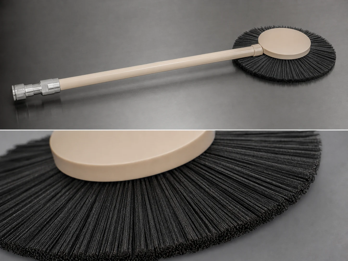
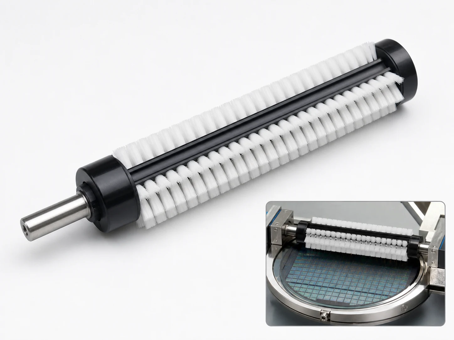
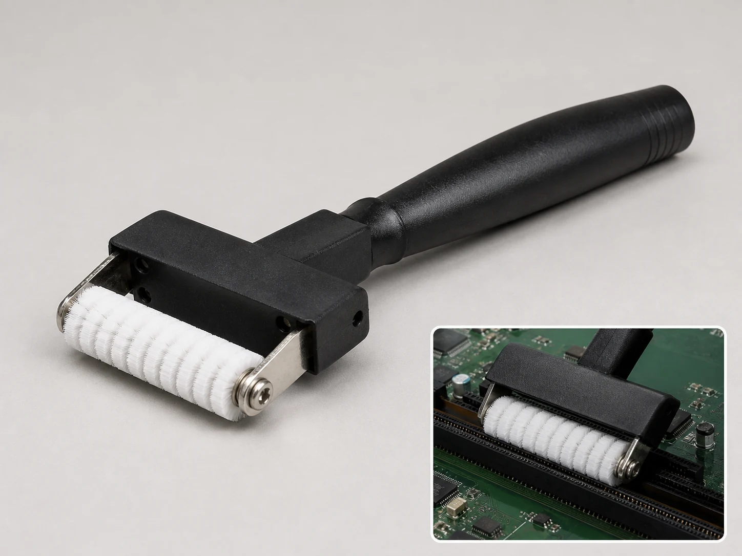
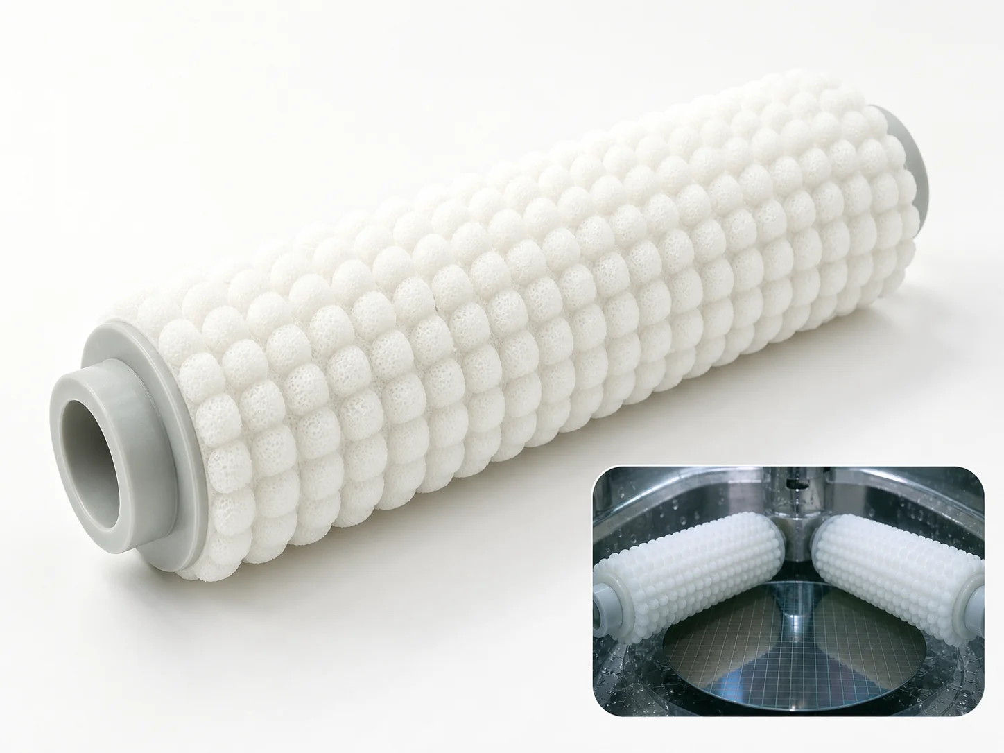
In precision processes, a brush can fail by shedding particles, marking the surface, carrying contamination or creating uncontrolled static. Start with those risks.
Wafer and precision substrates may require very low-contact-pressure materials or sponge-type cleaning rather than conventional bristles.
Specify whether the process has cleanroom, particle-shedding or material-extractable requirements.
PVA and wet-cleaning systems behave differently from dry dust-removal or static-control brushes.
Rollers, discs and plate brushes need exact OD, width, shaft or base geometry to maintain controlled contact in the machine.
A PVA wafer roller is selected around wet contact and surface protection, while a carbon-fiber equipment brush may address dry particles or static. Both are precision tools, but their cleaning mechanisms are not interchangeable.
Roller diameter, working width, sponge or filament material, core, shaft, base, contact profile and electrical properties can be tailored. Process drawings and cleanliness requirements are important inputs.
Send the substrate or equipment area, wet/dry process, contamination, cleanliness or ESD requirement and mounting dimensions. We can then assess the correct precision brush format.
Choose your brush type, cleaning task, material direction, and key details before sending a custom brush request.