Custom Cleaning Brush
Semiconductor Wafer PVA Cleaning Brush Roller
Tool-matched PVA sponge roller for post-CMP wafer scrubbers. Removes slurry particles without scratching. Custom OD, core, pore size, and nub pattern.
Medium brush
100 pcs
Minimum order
Worked with two hands or on a pole: chimney, gutter and pond-filter brushes, discs, cups and tank brushes.
Production lead time, once the specification is confirmed
- Up to 100 pcsWithin 7 days
- 101–5,000 pcsWithin 14 days
- 5,001–50,000 pcsWithin 21 days
- Over 50,000 pcsConfirmed with your quotation
Peak season can extend these times; the shipping date is confirmed in writing with your quotation. Sampling and shipping are quoted separately.
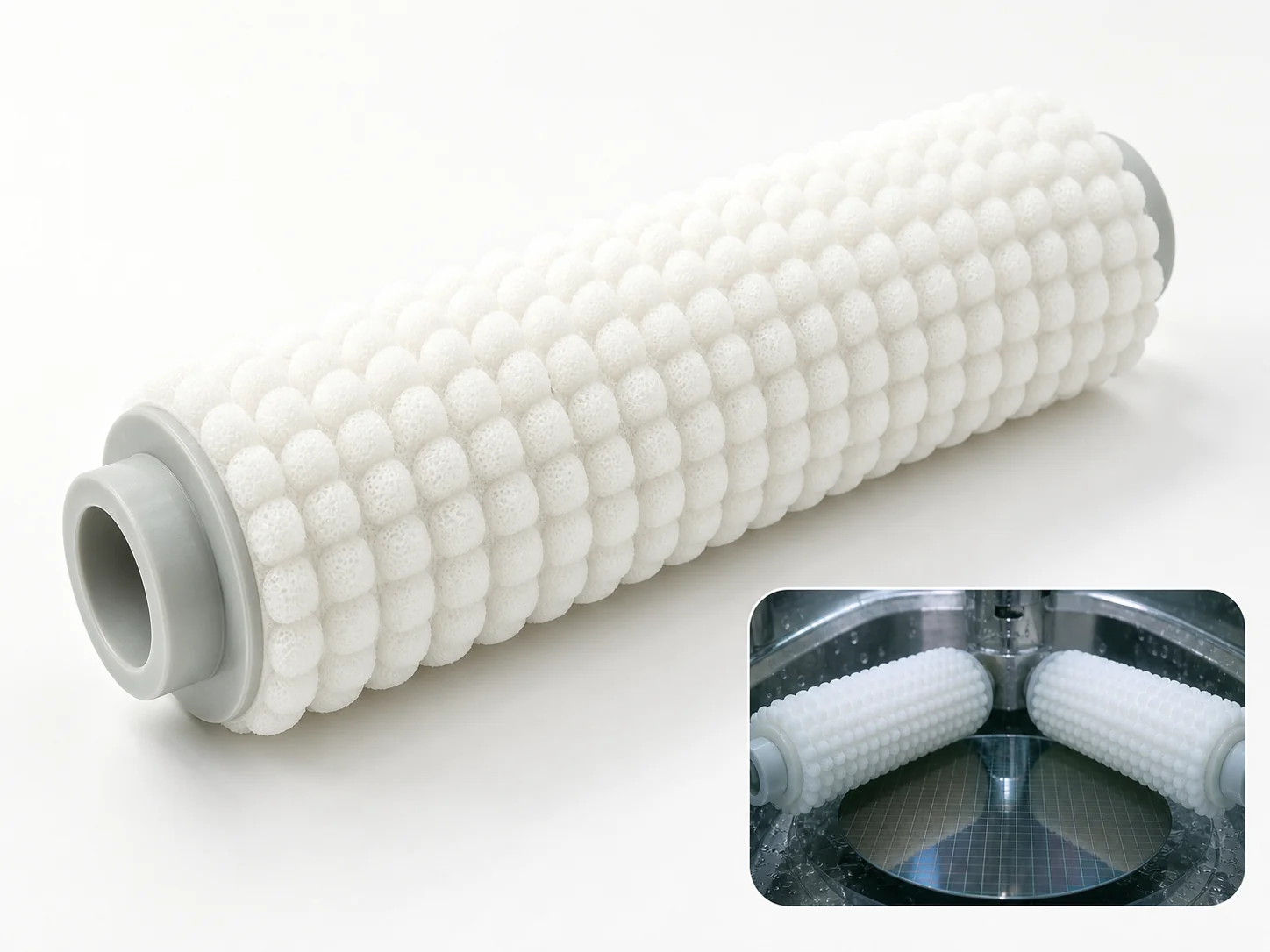
A hydrophilic PVA sponge roller that removes post-CMP slurry residue and particles from wafer front and back surfaces inside scrubber modules. The open-cell sponge and molded nubs provide non-scratching mechanical contact that works with DI water and dilute cleaning chemistries.
What can this brush do for you?
Removes slurry particles and post-CMP residue without scratching
Post-CMP wafers carry silica or ceria abrasive fines and loosened film residues. The PVA open-cell sponge body holds water and cleaning chemistry at the contact point, while the resilient nubs apply controlled wiping pressure across the wafer surface. The result is physical removal of small particles without the hard point contacts of nylon bristles or the cut risk of abrasive pads.
Adds almost no particles of its own
One of the main causes of recontamination in wafer scrubbers is the brush shedding material back onto the wafer. The cross-linked PVA sponge is designed for low particle release in wet operation. The open-cell structure lets removed slurry and loosened contamination flow into the rinse layer instead of being trapped in dense fiber bundles.
Maintains contact on flat and lightly patterned surfaces
The roller body compresses as it contacts the wafer, so the nub tips conform to minor surface height variation. This keeps contact pressure consistent across the die instead of concentrating force on high features. For patterned wafers, the compressibility can be tuned so the brush cleans the field without damaging delicate structures.
Works as part of the wet scrub sequence, not against it
The brush is designed to operate in DI water, dilute ammonia/peroxide, organic acid, or other approved cleaning chemistries at room to moderate temperature. Because the sponge absorbs and releases the liquid continuously during rotation, the mechanical action and chemical action stay coupled at the wafer surface.
Drops into existing scrubber modules
Roller OD, working length, core bore, and end fittings are matched to the scrubber tool model. The brush arrives ready to mount after hydration, so there is no modification of the cleaning module or custom shaft adapter required.
What is a Semiconductor Wafer PVA Cleaning Brush Roller?
A Semiconductor Wafer PVA Cleaning Brush Roller is a rotating cylindrical consumable installed in a wafer scrubber module. The outer layer is a molded PVA (polyvinyl alcohol) open-cell sponge formed with resilient surface nubs, and the center is a rigid core that slides onto the scrubber shaft or arbor.
During cleaning, the wafer passes between or beneath the rotating rollers while DI water or a cleaning solution is sprayed onto the contact zone. The wetted PVA nubs press against the wafer surface and remove slurry abrasives, pad debris, residual polishing film, and loose organic contamination from post-CMP and other wet-process steps. The used liquid carries the removed particles away from the surface.
Because PVA is a hydrophilic sponge, it must be fully hydrated before use. A dry roller is stiff and can damage the wafer or mark the surface. Once wet, the sponge becomes soft and compliant, which is what makes the contact non-scratching for bare silicon, oxide, copper, tungsten, and other wafer surfaces.
This product is a process consumable, not a general-purpose cleaning brush. It is not intended to replace chemical cleaning, to remove embedded or baked-on films, or to polish the wafer. It supports the wet cleaning sequence by providing controlled mechanical contact exactly where slurry particles and loose residue need to be displaced.
Technical Specifications
The table shows typical ranges for wafer scrubber PVA rollers. Final dimensions and PVA grade are selected from the tool platform, wafer size, and process recipe.
| Parameter | Value / Options |
|---|---|
| Working medium | PVA / PVF open-cell sponge, cross-linked for wet chemical exposure |
| Structure | Cylindrical roller with molded resilient nubs on the outer surface |
| Outer diameter | 50–100 mm, matched to the scrubber module gap and contact pressure |
| Inner diameter / core bore | 20–40 mm, matched to the tool shaft or arbor |
| Roller length | 150–450 mm, matched to wafer contact width and carrier travel |
| Pore diameter | 50–200 μm, selected for particle size, water retention, and release behavior |
| Nub pattern | Radial, helical, dot, or custom pattern; nub height and spacing per process |
| Core material | Stainless steel, aluminum, or polymer per module requirement |
| Operating condition | Wet process, room to moderate temperature, chemistry per specified PVA grade |
| Brush type | Custom Roller and Conveyor Brushes |
| How it is driven | Machine-driven, mounted in the equipment |
| Cleaning target | barrier cmp step, front-side and back-side wafer scrubbing, and bare wafer and reclaim cleaning |
| Surface or part | roller, bores, substrates, and pads |
| Residue or debris | particles, slurry, oxide, and polish |
| Mounting / connection | Shaft-Mounted / Flange |
All dimensions and grades can be adjusted to the tool drawing and process qualification data. If the scrubber module requires a different core ID, shaft key, or end hub configuration, those interfaces are specified at order time.
Where does this brush work best?
The primary use is post-CMP wafer cleaning, where the brush roller removes residual slurry abrasive from the wafer surface and bevel. This includes:
- Oxide, copper, tungsten, and barrier CMP steps in both single-wafer and batch scrubber tools.
- Front-side and back-side wafer scrubbing in double-sided brush scrubbers.
- Pre-diffusion, pre-epitaxy, and other particle-sensitive wet clean steps before thermal processes.
- Bare wafer and reclaim cleaning where non-scratching particle removal is required.
- Cleaning of other large flat or gently curved substrates that can tolerate wet sponge contact without aggressive abrasion.
For every application, the roller works with liquid at the contact point. It is not a dry brush and should not be run on a dry wafer surface.
How do I choose the right one?
Match the brush to the scrubber module first
Start with the tool model and module drawing. The outer diameter, roller length, core bore, and end fittings must match the shaft, drive, and wafer gap. A brush that fits mechanically but has wrong nub height or OD will change contact pressure and may leave residue bands across the wafer.
Select pore size for the residue and surface
Smaller pores hold more water in the contact zone and give a smoother, more compliant surface for fine slurry particles on bare or highly sensitive films. Larger pores release water and removed slurry more readily, which helps when residue loading is higher or particle size is larger. 50–200 μm covers most post-CMP applications, but the exact grade should be confirmed against the process recipe.
Set nub geometry for wafer topography
Flat bare wafers can use a lower nub height with dense contact. Patterned wafers with significant topography generally need a taller, more compressible nub so the roller cleans the field without pushing against isolated high features. Nub spacing also affects drainage and rinse removal.
Confirm chemical and temperature compatibility
PVA is offered in different cross-link densities for different cleaning chemistries. The wetted roller must survive the full operating recipe: chemical type, concentration, temperature, and total exposure time per day. If the process will run at elevated temperature or with aggressive oxidative mixtures, state this during selection.
Know when a different cleaning tool is the right answer
A PVA brush roller is not the right choice if the residue is a fixed film, hard scale, or requires aggressive polishing. For those cases, use the CMP process itself, a different brush medium, or an alternative wet clean such as megasonic or jet cleaning. PVA roller scrubbing is for loose particles and soft surface residue removal with controlled, non-scratching contact.
Can I customize this brush?
Semiconductor PVA cleaning brush rollers are usually tool-matched and process-qualified, so nearly every dimension and material property can be specified for the project. To start a custom configuration, provide the scrubber tool model, module drawing or shaft drawing, wafer size, process chemistry, temperature, particle size range, and target wafer count per roller. A sample roller or qualified reference also helps.
We can adjust:
- Roller dimensions — OD, length, core bore, end hub, shaft keyway, or other interface features.
- Nub geometry — height, width, spacing, pattern, and edge treatment.
- PVA grade — pore diameter, compressibility, water retention, and chemical resistance.
- Core material — stainless steel, aluminum, or polymer to match the tool and process compatibility.
- Hydration / pre-conditioning — factory pre-wetting, sealed packaging, or cleaning to specified particle level.
- Color and marking — identification ring, laser marking, lot traceability, or tool color coding.
- Packaging — cleanroom bagging, double bagging, individual sleeves, or bulk cassette packing.
For projects that require material declarations, lot inspection data, particle certifications, or third-party process testing, we can coordinate the necessary documentation and validation support during customization.
When is a semiconductor wafer PVA cleaning brush roller worn out rather than just dirty?
How should the PVA roller be prepared before installation?
Fully hydrate the roller in DI water or the specified process liquid before mounting and before wafer contact. A dry PVA sponge is stiff and can leave marks or damage the wafer. Soaking time depends on roller diameter and PVA grade; the roller is ready when the surface is uniformly soft and no dry core remains.
How can I tell when to replace the brush roller?
Monitor nub wear, surface degradation, and wafer defect trends. If the nub height is reduced beyond the process control limit, the sponge shows tearing or permanent flat spots, or the defect count on test wafers increases while all other tool parameters are stable, the roller should be replaced. Many fabs also set a fixed wafer-count replacement interval after qualification.
Does the brush roller replace chemical cleaning?
No. The roller supplies controlled mechanical contact that dislodges particles and thin residues. The cleaning chemistry and rinse flow still carry the loosened material away and prevent redeposition. For most post-CMP processes, the brush works as part of a sequence that includes chemistry, rinsing, drying, and often megasonic energy.
Can the same roller clean both sides of the wafer?
In double-sided scrubber modules, separate upper and lower rollers contact the front and back surfaces. In single-sided tools, the roller contacts one side at a time. The roller cannot clean both sides in one pass unless the module is designed for simultaneous top and bottom brushing. Specify the module configuration when ordering.
What should be checked during incoming inspection?
Check roller OD, length, and core bore against the tool drawing. Inspect the nub surface for tears, compressed areas, contamination, or foreign material. Verify the hydration state if pre-wetted rollers are required, and confirm lot identification matches the qualification record.
Can PVA rollers be used at high temperature?
PVA sponge has temperature limits that depend on the specific cross-link grade and cleaning chemistry. Standard wafer scrubber processes run at room to moderate temperature. If your process requires elevated temperature, the PVA formulation and core material must be selected for that condition. Do not assume a standard roller will survive a hot process without qualification.
Guides that go deeper on this
Abrasive Nylon Grit and Filament Selection
Read this guideGuideBrush Roller Conveyor Mistakes with Dry Dust
Read this guideGuideBrush Speed, Engagement, and Heat
Read this guideGuideConveyor Belt Cleaning Brush Design
Read this guideGuidePVA Sponge Roller Storage: Humidity and Temperature Control
Read this guideCustom Manufacturing RFQ
Describe Your Application
To quote this brush accurately, send the size, material, cleaning target, residue, quantity, and any available drawing or sample photo.
Drawing or photo optional — it speeds things up, it does not gate the enquiry.
Custom Brush RFQ
Send Your Brush Project
Upload a drawing, product photo, or sample photo and provide the core dimensions and cleaning conditions.
“We need a brush to remove wet residue from a stainless steel conveyor, about 800mm wide. The current brush wears quickly. We can send photos.”
“We sell drinkware and need a cleaning brush to include with the product. Quantity around 5,000 pieces.”