What Is a Semiconductor Brush?
A semiconductor brush is a specialized cleaning tool designed for use in semiconductor fabrication environments. It removes particles, process residues, and contaminants from surfaces such as silicon wafers, reticles, or process chamber components without leaving scratches, shedding particles, or introducing chemical contamination. These brushes are used in manual cleaning steps, as well as in automated wafer scrubbing and equipment maintenance procedures.
Common Types of Semiconductor Brushes
Understanding the main brush categories helps narrow the selection quickly:
- PVA Sponge Brush: Soft, absorbent polyvinyl alcohol foam brushes, commonly used in post-CMP wafer scrubbing. They conform to surfaces, trap particles, and are lint-free.
- Nylon Bristle Brush: Durable and chemically resistant, these are often used for cleaning metal equipment parts, load ports, and carriers. They can be anti-static if carbon-filled nylon is used.
- Microfiber Brush: Extremely soft and fine fibers for cleaning optical components, reticles, or delicate sensors. Minimal risk of scratching.
- Antistatic Brush: Made with conductive materials (e.g., carbon-filled nylon) to dissipate static charges and protect electrostatic discharge (ESD)–sensitive devices.
- Small-Area Swab Brushes: Miniature brushes or swabs for cleaning narrow trenches, corners, or tight geometries on wafers and reticles.
Comparison of Brush Structures and Materials
The table below summarizes the most common semiconductor brush types and their typical roles.
| Brush Type | Typical Use | Advantages | Limitations | Best Fit |
|---|---|---|---|---|
| PVA Sponge Brush | Post-CMP wafer cleaning, single-wafer scrubbing | Low particle shedding, high absorbency, soft | Limited solvent resistance; can degrade with strong acids | High-volume wafer cleaning lines |
| Nylon Bristle Brush (standard) | Equipment cleaning, carrier cleaning, manual station use | Chemical resistant, durable, good shape recovery | Can shed bristles if not properly manufactured; may scratch soft films | General fab equipment maintenance |
| Microfiber Brush | Reticle cleaning, optical inspection tool maintenance | Extremely low abrasion, excellent particle pickup | Not suitable for heavy contamination or strong solvents | Optics, reticles, sensors |
| Antistatic Brush (carbon-filled nylon) | Cleaning near bonders, test handlers, ESD-sensitive areas | Dissipates static, prevents ESD damage | Higher cost; slightly less durable than standard nylon | Packaging, test floors, assembly stations |
| Specialty PVA / Custom Shapes | Cleaning trenches, vias, or non-standard wafer topographies | Conforms to complex surfaces; can be designed to meet exact geometry | Longer production schedule; may require tooling | Advanced-node processes, custom scrubbing units |
How to Choose the Right Semiconductor Brush
Focus on these practical selection factors, not just cost or availability:
- Equipment Interface: Does your tool require a shank, a push-on handle, a quick-connect coupling, or a specific adapter? Mismatches cause downtime.
- Contact Surface Material: Brushing bare silicon, delicate low-k films, glass, or metal demands different hardness and abrasion limits.
- Residue Type: Determine whether you are removing loose particles, dried slurry, photoresist residue, or flux. Some residues require solvent-resistant materials.
- Cleanroom requirement and particle shedding: the required cleanroom level processes may require documented low particle generation and suitable packaging.
- Chemical Compatibility: Check the brush material’s resistance to your cleaning chemicals (IPA, DI water, acidic solutions, etc.).
- Replacement Cycle: Understand how long the brush lasts under your process conditions to plan inventory and preventive maintenance.
Operating Conditions That Affect Brush Selection
Beyond the basic fit, real-world conditions can narrow choices:
- Automated Scrubber Parameters: If your tool applies a specific downforce, rotation speed, or slurry flow, the brush must maintain integrity and not deform excessively.
- Static Control: In ESD-sensitive areas, non-conductive brushes can generate damaging static voltages. An antistatic brush is essential.
- Temperature and Humidity: Some PVA brushes soften in high-temperature DI water; check specifications if your process runs above 40 °C.
- Cleanroom Packaging: Brushes used in ISO the required cleanroom level–5 areas should come double-bagged and have documented low particle test results.
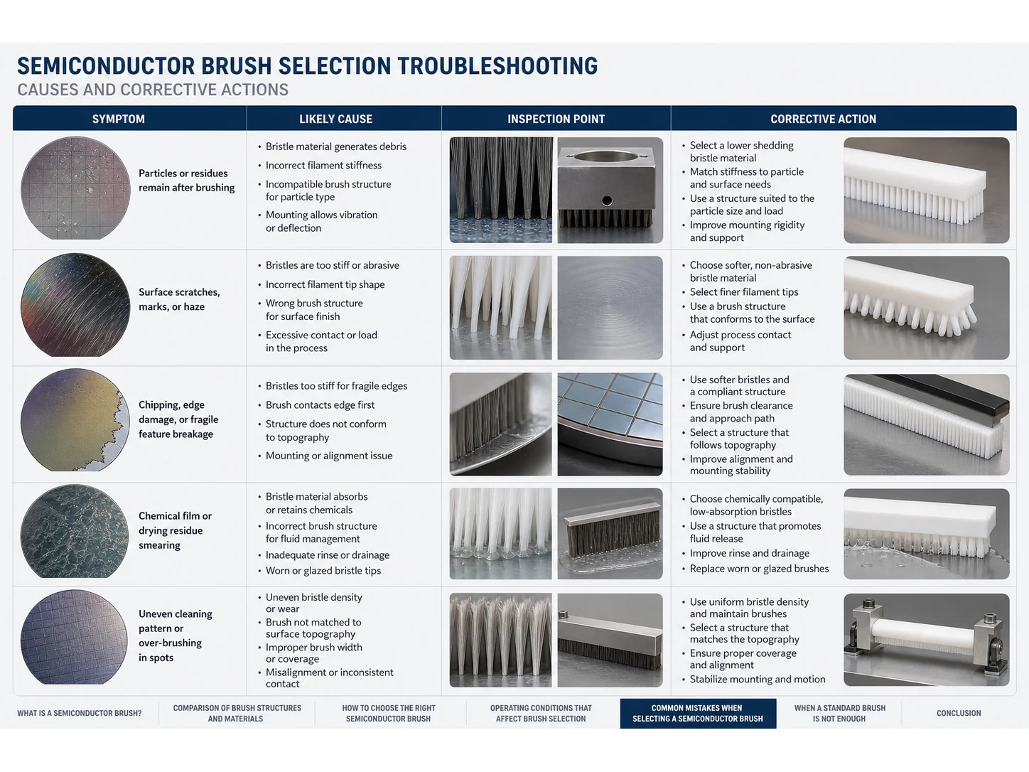
Common Mistakes When Selecting a Semiconductor Brush
- Choosing by cost alone: A cheaper brush that sheds particles or scratches wafers causes far higher costs from yield loss.
- Ignoring bristle shedding characteristics: In critical cleaning, shedding leads to re-contamination and electrical shorts.
- Using a brush that is too hard: Abrasive brushes can damage low-k dielectric films or polished metal surfaces.
- Assuming one brush works for every residue: Different residues require different material attributes; a brush optimized for slurry may not handle organic residues well.
- Overlooking mounting detail: Even a high-quality brush fails if it does not fit the chuck or quick-connect correctly.
- Skipping validation in the actual process: Always test a sample brush with in-line particle monitoring and wafer inspection before full deployment.
When a Semiconductor Cleaning Brush Is the Wrong Choice
Standard semiconductor brushes cover most common cleaning tasks, but several situations demand a custom approach:
- Non-standard equipment interfaces: If your tool uses a proprietary chuck or holder, off-the-shelf brushes will not fit securely. A custom drawing and sample approval become necessary.
- Unique geometry requirements: Cleaning deep trenches, angled surfaces, or complex 3D structures may require a custom brush with specialized bristle arrangement, angles, or materials to reach all surfaces effectively.
Conclusion
Selecting a semiconductor brush is a process-critical decision that should involve engineering evaluation, not just procurement. By matching the brush to the equipment, residue, surface, and cleanroom requirements, you minimize particle contamination and support process consistency after validation. Whenever possible, test brush samples under real process conditions with appropriate metrology before committing to a full supply.
Bottom Line
The best result comes from matching semiconductor cleaning brush selection: materials, contamination risk, and validation to the real cleaning task rather than forcing one brush to solve every condition. Confirm access, residue, surface limits, and replacement routine first; then use a small trial or inspection step before scaling the method into daily work.
Frequently Asked Questions (FAQ)
1. What is the best brush material for post-CMP wafer cleaning?
PVA sponge brushes are commonly considered for post-CMP cleaning because they are soft, absorbent, and can support particle-control goals when the material, surface contact, chemistry, and cleaning process are validated together. They should still be tested under the actual wafer-cleaning conditions rather than selected by material name alone.
2. How do I know if I need an antistatic brush?
If your cleaning process involves ESD-sensitive components or takes place in an area where static discharge could damage devices, a static-control brush may be needed. These brushes are typically made with conductive or dissipative materials like carbon-filled nylon, which help control static when they are used with a suitable ESD-control process.
3. Can I use the same brush for different cleaning chemicals?
Not always. You must verify the brush material’s chemical compatibility with each solvent or solution used. For example, some PVA brushes degrade with strong acids or certain organic solvents, while nylon bristles offer broader resistance. Always check the manufacturer’s chemical compatibility chart and test under actual conditions.
4. What information should I provide before requesting a semiconductor cleaning brush?
Provide the process step, wafer or component type, cleaning chemistry, target residue, brush contact method, equipment interface, and any particle-control, ESD-control, or documentation requirements. The more specific the process context is, the less the supplier has to guess.
5. Is a cleanroom brush automatically suitable for semiconductor use?
No. “Cleanroom” is only a starting point. Semiconductor cleaning also depends on material shedding, chemical compatibility, surface contact, packaging, handling, and whether the brush has been tested in the actual cleaning process.
6. When should sample testing be done?
Sample testing should be done before production use when the surface is high value, the process uses chemicals, ESD risk exists, or particle contamination would create downstream problems. A small controlled trial is usually more useful than choosing only from a material name.
Technical References
- NISTIR 4653 — Metrology for the Semiconductor Industry
- ISO 14644-1 Cleanrooms and Associated Controlled Environments
Which bristle material fits this job — Nylon PA, PVA Sponge or Microfiber?
| Material | Continuous temperature (°C) | Peak temperature (°C) | Water absorption | Hardness |
|---|---|---|---|---|
| Nylon PA | 93 | 121 | 0.3–9% by PA grade and conditioning | Medium to firm; filament diameter and trim length control bending force. |
| PVA Sponge | 60 | 90 | — | Soft absorbent contact material; hardness/compression is controlled by foam or sponge density. |
| Microfiber | 80–120 | 140–170 | 0.2–1.0%Material Itself ; Structure Can Absorb 3–7 Times Its Own Weight | — |
Figures as published by Brushtec / DuPont. Confirm the exact grade against the supplier datasheet before ordering.
What should replace Nylon PA when it stops working?
- Nylon PA — Compare Nylon PA with PP, PBT, PET. Change material when wet stiffness, temperature, chemical resistance, conductivity, particle shedding, or surface marking becomes the limiting factor.
- PVA Sponge — Compare PVA Sponge with PU sponge, PP sponge, microfiber. Change material when wet stiffness, temperature, chemical resistance, conductivity, particle shedding, or surface marking becomes the limiting factor.
- Microfiber — Compare Microfiber with Cotton yarn, wool, felt, soft PBT filament. Change material when wet stiffness, temperature, chemical resistance, conductivity, particle shedding, or surface marking becomes the limiting factor.