What Is a Wafer Cleaning Brush?
A wafer cleaning brush is a rotating or oscillating brush designed for direct contact cleaning of silicon wafers and other semiconductor substrates during fabrication. Its primary task is to physically dislodge particles while minimizing surface damage, chemical interaction, and recontamination. These brushes are typically mounted in wet bench or single‑wafer cleaning tools and must meet strict purity, durability, and contamination control standards specific to fab environments.
Common Types of Wafer Cleaning Brushes
Wafer cleaning brushes fall into a few main categories based on the contact material:
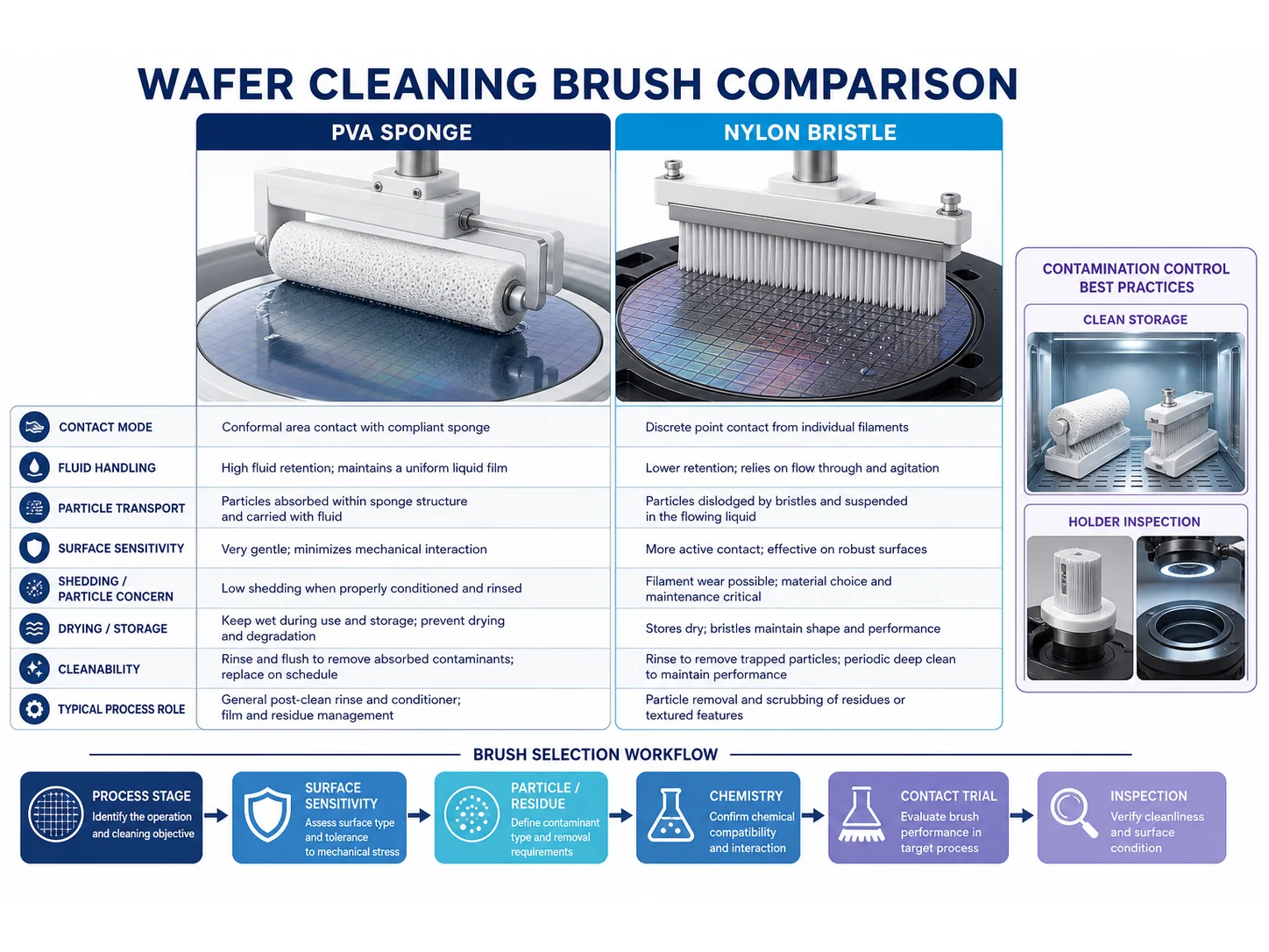
- PVA Sponge Brushes – Made from open‑cell polyvinyl alcohol foam; known for soft, conformal contact and high absorbency.
- Nylon Bristle Brushes – Use fine nylon filaments; offer more aggressive mechanical scrubbing action.
- Mohair and Specialty Brushes – Sometimes used for niche applications but less common in high‑volume semiconductor manufacturing.
For most post‑CMP and general wafer cleaning applications, the decision usually comes down to PVA sponge versus nylon bristle.
PVA Sponge vs Nylon Bristle: Key Comparison
| Factor | PVA Sponge Brush | Nylon Bristle Brush | What to Confirm |
|---|---|---|---|
| Contact Behavior | Soft, conformal contact; deforms to follow surface topography, reducing point pressure. | Discrete bristle tips; can reach into recesses but may concentrate force on small areas. | Sponge compression modulus; bristle diameter, density, and tip geometry. |
| Particle Control | Absorbs particles into the sponge matrix; risk of re‑deposition if not properly rinsed. | Mechanically sweeps particles away; bristle stiffness can generate fine debris if not designed for cleanroom use. | Particle shedding data (e.g., liquid particle test results after extended soaking); sponge rinsibility. |
| Chemical Exposure | Sensitive to strong acids, alkalis, and solvents; can swell, degrade, or leach extractables. | Generally better chemical resistance; nylon can hydrolyze in very hot or extreme pH environments. | Chemical compatibility chart for full process bath; extraction test results for leachables. |
| Surface Sensitivity | Excellent for polished, bare silicon and fragile low‑k films; low risk of microscratching. | May cause surface damage on soft or delicate layers; better suited for robust substrates or rugged pre‑clean steps. | Scratch test data on relevant film stacks; SEM review after processing. |
| Process Validation | Often validated for standard CMP clean; may require conditioning cycles to stabilize performance. | Can require more extensive qualification due to bristle wear and potential for particle generation over life. | Supplier‑provided endurance/lifecycle data; in‑house defect density trend monitoring. |
How to Choose the Right Wafer Cleaning Brush
Selection should start with a clear understanding of the process and substrate. Key decision factors include:
- Substrate material – Bare silicon, patterned wafers, or sensitive low‑k/ metal layers.
- Contaminant type – Slurry particles, organic residues, or tenacious post‑etch debris.
- Chemical environment – pH range, solvent exposure, and bath temperature.
- Tool compatibility – Brush dimensions, mounting, rotation speed, and oscillation limits.
- Consumable life – Expected number of wafers per brush before replacement or re‑conditioning.
Before finalizing a brush, request the following from suppliers:
- Material safety data sheet (MSDS) for the brush material.
- Particle shedding test results (e.g., liquid particle test result, TXRF analysis of rinse water).
- Chemical leachables/extractables data for your specific chemistry.
- Mechanical endurance and compression set data over expected life.
- References or case studies for similar applications (without proprietary details).
Always run an in‑house qualification using actual process chemistry and wafer types to verify defect performance.
Setup and Process Factors That Influence Brush Performance
Even the best brush underperforms if not set up correctly. Parameters that must be tuned to the brush type include:
- Brush pressure – Too high can damage wafers; too low reduces cleaning efficiency.
- Rotation speed and oscillation – Must match the brush’s mechanical tolerance and cleaning action.
- Chemical flow and rinse – Adequate flow is essential to carry away dislodged particles, especially for PVA sponges that can re‑deposit if starved.
- Brush conditioning – Many PVA brushes require a break‑in run to saturate and stabilize before production use.
Common Mistakes When Selecting Wafer Cleaning Brushes
- Treating general cleaning brushes as semiconductor‑process brushes. Industrial nylon brushes may contain fillers, oils, or metal residues that contaminate wafers. Only use brushes designed and packaged for cleanroom environments.
- Selecting based on cost or catalog spec alone. A low‑cost brush that requires frequent replacement or causes yield loss is far more expensive overall.
- Ignoring chemical compatibility data. Even “chemically resistant” nylon can swell or leach at high temperatures or in strong solvents; always verify with your exact chemistry.
- Skipping the brush break‑in procedure. Unconditioned PVA sponges may shed heavily in the first few wafers, leading to false defect spikes.
- Not re‑validating when changing any process variable. A new slurry, different rinse chemistry, or even a slight temperature shift can alter brush performance and risk quality.
When a Standard Wafer Cleaning Brush Is the Wrong Choice
Standard PVA or nylon brushes may fall short in several situations:
- Advanced nodes with sub‑10 nm defect targets – Tighter defect budgets often demand custom brush designs, ultra‑high‑purity materials, or non‑contact alternatives.
- High‑aspect‑ratio structures – Brush bristles or sponge may not effectively clean deep trenches or vias; megasonic or spray cleaning can be more suitable.
- Extremely fragile films – If even PVA sponge contact causes damage, consider cryogenic aerosol cleaning or laser‑based methods.
- Aggressive chemistries – For processes using concentrated acids at elevated temperatures, standard brush materials may degrade; specialty engineered polymers may be required.
In these cases, work directly with your equipment supplier or a qualified consumables partner to co‑develop a solution. Full metrology validation (SEM review, surface defect inspection, electrical test) is mandatory before introducing a new brush type into production.
Final Takeaway
The choice between a PVA sponge and a nylon bristle wafer cleaning brush comes down to the balance between mechanical cleaning efficiency and surface protection. PVA sponge brushes excel in gentle, low‑defect cleaning for polished and fragile wafers, while nylon bristles provide the scrubbing action needed for tougher residues. Always ground your selection in validated material data and in‑house process testing rather than generic claims or assumptions.
Frequently Asked Questions
What is the main advantage of a PVA sponge brush over nylon for wafer cleaning?
PVA sponge brushes provide a soft, conformal contact that dramatically reduces the risk of microscratches on bare silicon, polished surfaces, and fragile films. Their open‑cell structure also absorbs and entraps particles, minimizing re‑deposition during cleaning.
Can nylon bristle brushes be used on patterned wafers?
Yes, but with caution. Nylon bristles can reach into recesses and clean around structures better than a sponge in some cases. However, the bristles must be fine enough and designed for the specific pattern density to avoid damaging delicate features. Always test on non‑production wafers first.
How do I know if a brush is truly semiconductor‑grade?
A semiconductor‑grade brush should be manufactured in a cleanroom environment, packaged to prevent contamination, and accompanied by a certificate of conformance that includes purity data (metal ion content, particle test results), chemical compatibility test results, and often lot traceability. Avoid brushes labeled only for “industrial” or “precision cleaning” without fab‑specific documentation.
What chemical compatibility data should I request from a brush supplier?
Request extraction test data (leachables and extractables) for the specific chemicals and temperatures you use, along with long‑term immersion stability results. Ask for pH and solvent resistance charts, and confirm that the brush material does not degrade into particulates that can contaminate the wafer or process bath.
How often should wafer cleaning brushes be replaced?
Replacement frequency depends on brush type, process chemicals, pressure, and wafer throughput. It is typically determined through in‑house endurance testing — monitoring defect counts, brush wear, and cleaning uniformity over time. Many fabs establish a preventive maintenance schedule based on wafer count or visual inspection criteria.
Can I use the same brush for different cleaning chemistries?
Not without verification. A brush that works well in a mild alkaline cleaner may swell, leach, or mechanically fail in an acidic or solvent‑based process. Cross‑contamination risks also increase. Ideally, dedicate brushes to a single chemistry or fully validate a brush across all intended chemicals before mixing.
What testing should I perform before implementing a new brush in my process?
At minimum, run: a particle performance test (add defect counts before and after cleaning on monitor wafers), a chemical compatibility soak test, a wafer scratch evaluation using SEM or optical inspection, and a brush lifetime test to measure cleaning efficiency decay. Process engineers should also check for any recipe adjustments needed in the cleaning tool.
Are there alternatives to physical brushes for wafer cleaning?
Yes. Non‑contact methods such as megasonic agitation, high‑pressure spray, cryogenic aerosol cleaning, and laser‑induced shock cleaning can be used when brush contact poses a risk. However, these methods may not match the particle removal efficiency of a physical brush for some residues, so the choice depends on defect tolerance and substrate fragility.
Technical References
- NISTIR 4653 — Metrology for the Semiconductor Industry
- ISO 14644-1 Cleanrooms and Associated Controlled Environments
- British Plastics Federation — Thermoplastics
Which sponge and foam grade fits this job — PVA Sponge, PU Sponge or PU Foam?
| Grade | Continuous temperature (°C) | Peak temperature (°C) | Water absorption | Hardness |
|---|---|---|---|---|
| PVA Sponge | 60 | 90 | — | Soft absorbent contact material; hardness/compression is controlled by foam or sponge density. |
| PU Sponge | 80 | 110 | — | Soft absorbent contact material; hardness/compression is controlled by foam or sponge density. |
| PU Foam | 80–100 | 110–130 | Open-Cell Structure Can Absorb 5–30 Times Its Own Weight; Polymer Itself 1–5% | Shore OO 20–80 or Shore A 10–40 |
| Melamine Foam | 150–180 | 200–240 | Open-Cell Structure Can Absorb 10–40 Times Its Own Weight | Shore OO 20–60 |
Figures as published by Material manufacturer TDS / ISO / ASTM / industry reference. Confirm the exact grade against the supplier datasheet before ordering.
What should replace PVA Sponge when it stops working?
- PVA Sponge — Compare PVA Sponge with PU sponge, PP sponge, microfiber. Change material when wet stiffness, temperature, chemical resistance, conductivity, particle shedding, or surface marking becomes the limiting factor.
- Nylon PA — Compare Nylon PA with PP, PBT, PET. Change material when wet stiffness, temperature, chemical resistance, conductivity, particle shedding, or surface marking becomes the limiting factor.