Custom Cleaning Brush
PCB Brush
Conductive nylon PCB brush for static-safe cleaning of boards, edge connectors, and optical surfaces. Head widths 3-40 mm, filaments 0.05-0.30 mm.
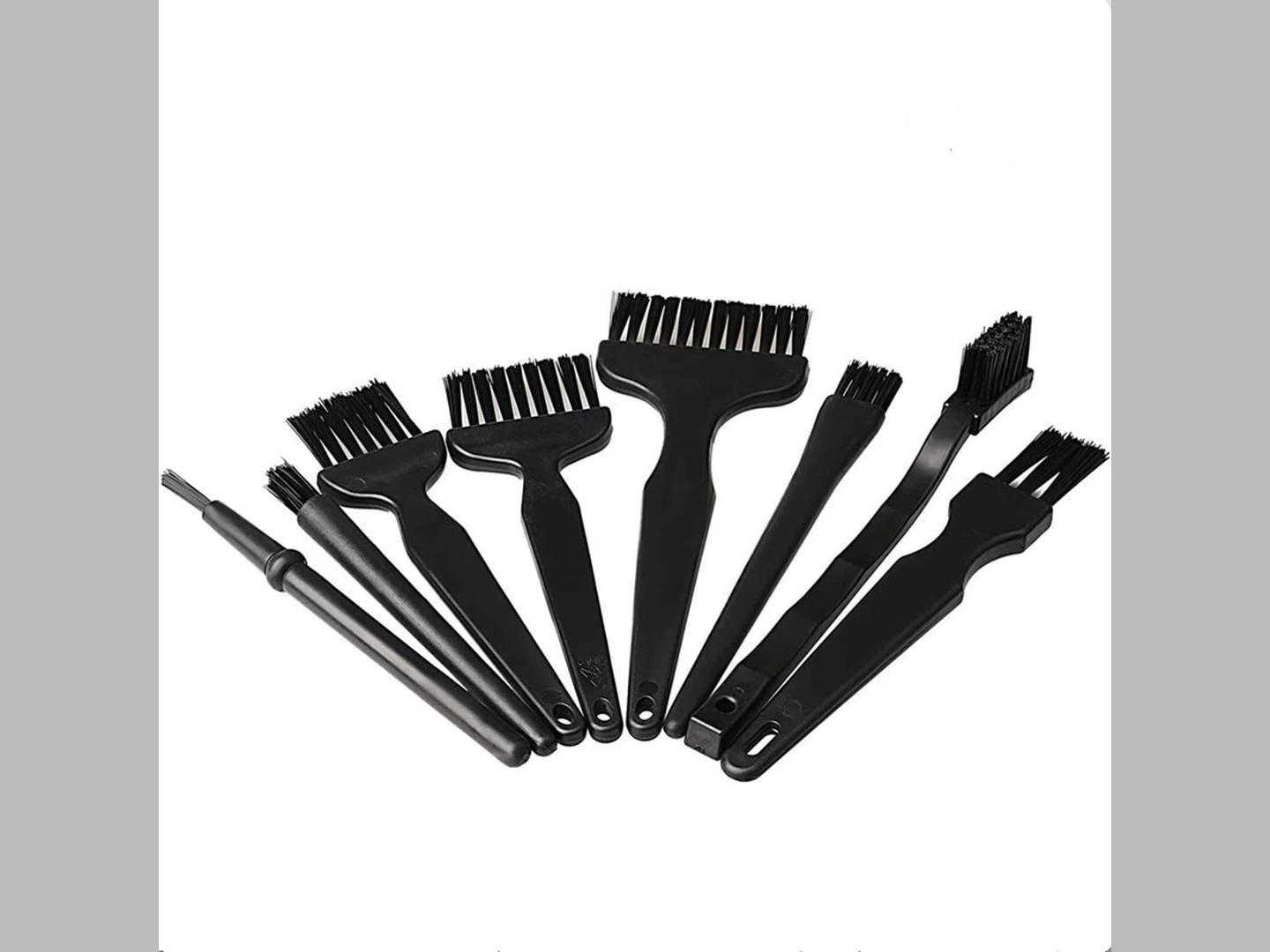
Small brush
500 pcs
Minimum order
Held in one hand: tube, bottle, detail and swab brushes — including long-handled ones with a small head.
Production lead time, once the specification is confirmed
- Up to 500 pcsWithin 7 days
- 501–50,000 pcsWithin 14 days
- Over 50,000 pcsWithin 21 days
Peak season can extend these times; the shipping date is confirmed in writing with your quotation. Sampling and shipping are quoted separately.
A handheld ESD-safe PCB brush built with conductive nylon filaments for removing dust, lint, solder particles, and light flux residue from printed circuit boards, edge connectors, and precision electronic assemblies without building a static charge. Head widths from 3 to 40 mm and filament diameters from 0.05 to 0.30 mm let one brush family cover fine-pitch component rows, connector slots, and broader board surfaces.
What can this brush do for you?
Keeps Static Off the Board Instead of Building It
Ordinary nylon and natural-fiber brushes generate triboelectric charge as the filaments slide across the board. This brush uses carbon-loaded conductive nylon with a surface resistivity between 10³ and 10⁹ Ω, and the filament mass continues through a conductive ferrule into a dissipative handle. When the operator is grounded, the charge has a controlled path to leave the brush instead of discharging into an adjacent component.
Reaches Between Tall Components and Into Slot Contacts
Head widths start at 3 mm and filament diameters go down to 0.05 mm, so a narrow row of filaments can pass between capacitors, connectors, and fine-pitch leads without bending components or flattening the brush face. The same profile reaches into card-edge slots, pin headers, and test-point fields where a wide brush would only polish the top surface.
Removes Lint and Particles Without Abrading Plating
Conductive nylon PA filaments are softer than solder mask, copper, nickel, and gold-plated contact surfaces. They lift dust, fiber lint, oxide particles, and light no-clean flux film with the filament tips rather than cutting into the surface. This matters most on gold edge fingers and optical end faces where a scratch changes contact resistance or signal quality.
Delivers a Consistent Working Face for Repeatable Passes
Filaments are set at a controlled density and precision-trimmed, so the same brush performs the same contact across every board in a lot. Maintenance and production engineers do not have to re-qualify a cleaning step because the tool changed its contact pattern halfway through a run.
Scales From Bench to Automation
Overall lengths from 100 to 200 mm fit one-handed rework, while the same filament and head geometry can be built onto a machine shank or fixture mount for automated inline cleaning. A single qualification can carry from manual prototype work to repeatable production strokes.
What is a PCB Brush?
A PCB brush is a small handheld or fixture-mounted cleaning tool whose working face is made from conductive nylon filament rather than standard insulating nylon, hair, or natural fiber. In electronics assembly, the material choice is the product: when an insulating brush sweeps a board, friction separates charges and the brush face can hold a potential high enough to damage ESD-sensitive components. The conductive filament mass gives that charge a controlled path to a grounded handle, wrist strap, or workstation instead of letting it accumulate at the tips.
In practice, the brush is used close to the board: along solder-side traces, around SMD component bodies, through connector pin fields, and inside card-edge slots. It is normally a dry cleaning tool, but light wiping with a compatible solvent such as IPA can be used after the brush has removed loose particulate. Filament diameter and trim length set the access and stiffness. A 0.05 to 0.10 mm filament follows fine-pitch detail and enters narrow slots; a 0.20 to 0.30 mm filament carries more beam strength for wider open zones and heavier dust. Head width is chosen for the zone being cleaned, not for the whole board: most PCB brushes are used for local treatment of a specific row, connector, or edge.
This is not a heavy scrubbing brush and it does not replace solvent-based flux removal. Hardened rosin, cured conformal coating, and heavy oxide accumulations require a different process. The PCB brush is for particulate control and light film removal on static-sensitive surfaces where the contact method must not introduce another hazard.
Technical Specifications
| Parameter | Value / Options |
|---|---|
| Product form | Handheld ESD-safe PCB cleaning brush; fixture or machine-shank versions available |
| Head width | 3 to 40 mm, selected to the smallest access gap or connector span |
| Overall length | 100 to 200 mm, set for bench reach or automated stroke length |
| Filament diameter | 0.05 to 0.30 mm; finer for fine-pitch and slots, heavier for open board areas |
| Trim length | 8 to 25 mm, adjusted for slot depth and stiffness |
| Fill material | Conductive nylon PA, carbon-loaded or equivalent ESD formulation |
| Surface resistivity | 10³ to 10⁹ Ω, project-selectable within the dissipative-to-conductive range |
| Handle / ferrule | Conductive or dissipative polymer, conductive anodized aluminum, or ESD-safe overmold |
| Grounding interface | Continuous conductive path from filament mass through ferrule and handle to a grounded operator, mat, or fixture |
| Operating environment | Dry or light solvent-assisted cleaning; material grades matched to process temperature and chemical exposure |
| Brush type | Custom Handheld Detail Brushes |
| How it is driven | Hand-guided |
| Cleaning target | smt and through-hole assembly line, card-edge connector and pin header, and optical end face and lens carrier cleaning |
| Surface or part | boards, connectors, slots, edges, pins, fixtures, optical end faces, and precision housings |
| Residue or debris | dust, flux, particles, lint, fiber, flux residue, oxide, and fiber lint |
| Mounting / connection | Continuous conductive path from filament mass through ferrule and handle to a grounded operator, mat, or fixture |
Final dimensions and resistivity are set against your board layout, minimum access gap, contamination type, and workstation grounding scheme. The ranges above are the standard configuration window; final values are specified per order.
Where does this brush work best?
- SMT and through-hole assembly lines: removing solder balls, fiber lint, and dust from populated boards before automated optical inspection, conformal coating, or final test.
- Card-edge connectors and pin headers: narrow multifilament heads enter slots and clear oxide particles and lint from mating surfaces before insertion.
- Optical end faces and lens carriers: fine conductive filaments remove polishing particles and static-attracted dust from end faces and coated optics when a soft, low-pressure pass is specified.
- Rework and repair benches: sweeping loose flux residue, solder particles, and fiber debris from reworked joints before cleaning or continuity checks.
- Test fixtures, probe cards, and precision housings: keeping contact surfaces and seating areas free of dust that changes contact resistance or dimensional stack-ups.
How do I choose the right one?
Start with the smallest opening and the most sensitive surface in the cleaning path, then work outward.
Measure the access gap. Identify the narrowest gap between components or the smallest slot that must be entered. The head width must be slightly smaller than that gap, with enough filament length to reach the surface at the bottom. If the brush cannot enter without bending component leads, go narrower.
Match filament diameter to the detail level. For fine-pitch ICs, 0.5 mm connectors, and optical end faces, use 0.05 to 0.10 mm filaments with a narrow head. For general board dusting and edge contacts, 0.10 to 0.15 mm is a balanced choice. For open copper planes and heavier particulate, 0.20 to 0.30 mm filaments provide more sweep force and longer wear.
Select the resistivity for the ESD control plan. A dissipative range around 10⁶ to 10⁹ Ω bleeds charge more gently and is common where the brush may approach sensitive components. A conductive range around 10³ to 10⁵ Ω drains charge faster and may be preferred for heavily charged processes or where the workstation standard requires it. Either way, the handle, operator, and fixture must provide a continuous path to ground; the filament resistivity is only part of the circuit.
Decide how the brush will be held. A 100 to 150 mm handle suits close rework and inspection; 150 to 200 mm lengths give more reach for inline stations. For automated strokes, specify the machine shank, clamping area, or mounting thread so the brush repeats its position cycle after cycle.
| Cleaning situation | Suggested configuration |
|---|---|
| Fine-pitch SMD rows and connector slots | 3 to 10 mm face, 0.05 to 0.10 mm filament, dissipative handle |
| General board dusting and edge connectors | 10 to 20 mm face, 0.10 to 0.15 mm filament |
| Open board areas before coating | 20 to 40 mm face, 0.20 to 0.30 mm filament |
| Static-critical optics and precision housings | Narrow face, fine filament, low contact pressure, grounded fixture |
Know when a PCB brush is not the solution. Hardened or polymerized flux, cured adhesive residue, and heavy oxidation call for solvent cleaning, ultrasonic or spray-in-air systems, or an abrasive brush made from glass fiber or another accepted material for the specific process. Do not use conductive-filament brushes on energized boards, and do not use them where coarse filaments would bend fine leads. If the target is a through-hole or deep socket, a tube or specialty probe brush may be the better geometry.
Can I customize this brush?
Most PCB brushes are ordered against a specific board or station, so the brush is built from a variable geometry rather than taken from a fixed catalog size. To define a custom configuration, we need the board zone drawing or photo, the smallest access gap, the components or connector style, the type of residue, the surface finishes involved, the target ESD resistance, and how the brush will be held or mounted.
From there we can adjust:
- Head geometry: width, trim length, flat, angled, or contoured face, single or double filament rows, and special profiles for slots or pin fields
- Filament system: diameter, density, conductive nylon grade, resistivity range, trim pattern, and stiffness
- Handle and ferrule: conductive or dissipative polymer, anodized aluminum, overmold, length, shape, and grounding connection style
- Machine interface: plain shank, hex, threaded, clamping block, or fixture insert for automated strokes
- Identification: laser marking, pad printing, color coding by resistivity or station, and customer part numbers
- Packaging: bulk, individual ESD-safe pouch, tray for automation, or project-specific packing
If your project requires material declarations, resistivity test data, inspection reports, or support for third-party qualification, we can supply the documentation and testing coordination during the customization phase.
Which filament survives the cleaning and still lasts on a PCB brush?
How can I verify that the brush is still ESD-safe?
Use a surface resistance meter or megohmmeter across the filament tips and the handle or ground point. The reading should fall within your specified 10³ to 10⁹ Ω range. If the meter shows an open circuit, inspect for a broken conductive path at the ferrule or handle junction, a cracked handle, or a filament mass that has become coated with insulating residue. Re-check after cleaning.
Can I clean the brush with isopropyl alcohol?
Light IPA wiping is generally compatible with conductive nylon PA, but the brush should be allowed to dry before returning to the ESD workstation. Do not soak the handle junction or expose it to strong acids, hot alkaline solutions, or aggressive solvents without first confirming the specific material grade. Solvent compatibility should be part of the specification if wet cleaning is planned.
Will conductive nylon filaments scratch gold-plated contacts or optical surfaces?
Under normal hand pressure, conductive nylon is softer than gold plating, copper, nickel, and most optical coatings, so the filaments themselves will not scratch the surface. The larger risk is hard particles trapped in the filament mass from a previous job. Inspect and clean the brush before using it on optical end faces or gold fingers, and use a dedicated brush for critical surfaces.
Can I use this brush on a powered board?
No. Conductive and dissipative brushes are meant for de-energized assemblies. If the filament or handle contacts a live trace, the conductive path can carry current to the operator or fixture and damage the board. De-energize and follow lockout/tagout procedures before cleaning.
What does the brush remove, and what does it not remove?
It removes dry particulate, fiber lint, solder balls, oxide dust, and light flux film by mechanical contact. It does not dissolve or strip hardened rosin flux, cured adhesive, or heavy contamination. Those conditions need a solvent process, ultrasonic or spray cleaning, or an abrasive tool selected for the specific surface and process.
How do I know when to replace the brush?
Replace when the trim no longer stands upright, filaments bend and stay bent, the face becomes matted or uneven, or surface resistivity drifts outside the specified range. In high-mix production, a visual check under magnification at the start of each shift is more useful than a fixed replacement schedule.
Guides that go deeper on this
How to Choose the Right PCB Brush for Static-Sensitive Parts
Read this guideGuidePCB Brush Mistakes on Precision Carriers
Read this guideGuidePCB Brush vs Standard Brushes: Static-Sensitive Parts
Read this guideGuidePCB Brush: Specs for PCB Dust Removal
Read this guideGuidePCB Cleaning Brushes: ESD Control and Low-Residue Materials
Read this guideCustom Manufacturing RFQ
Describe Your Application
Please share the brush dimensions, working area, residue type, material direction, quantity, and a drawing or photo for quotation.
Drawing or photo optional — it speeds things up, it does not gate the enquiry.
Custom Brush RFQ
Send Your Brush Project
Upload a drawing, product photo, or sample photo and provide the core dimensions and cleaning conditions.
“We need a brush to remove wet residue from a stainless steel conveyor, about 800mm wide. The current brush wears quickly. We can send photos.”
“We sell drinkware and need a cleaning brush to include with the product. Quantity around 5,000 pieces.”